Nvidia and TSMC allegedly tape out next-gen 14nm Pascal GPU

by Mark Tyson on 8 June 2015, 12:06

Tags: NVIDIA (NASDAQ:NVDA), TSMC

Quick Link: HEXUS.net/qacr2z

Add to My Vault: x

According to sources on the Beyond3D and 3DCenter forums Nvidia's next-gen Pascal GPU has been taped out. Thus the first of the Pascal architecture chips, known as the GP100, has successfully been prototyped using the TSMC 16nm FinFET Plus process. This is a significant milestone and now engineers will be able to test and tweak the design to ready it for market rollout.

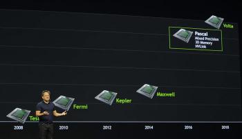
As trailed by Nvidia, at its GTC Keynote this March, the Pascal GPU will be "10X faster than Maxwell". While that was admittedly a rough high-level estimate, and applied to niche purpose 'deep learning' calculations, it does at least sound like a very significant performance jump. In more general perfromance terms the Pascal architecture will implement three important new features:

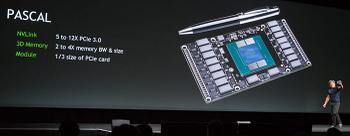
"One is mixed precision, which is provides at 3X the level of Maxwell. Another is 3D memory, which provides more bandwidth and capacity simultaneously. A third is NVLink, which is an ability for multiple GPUs to be connected at very high speeds. It also has 2.7X more capacity than Maxwell."

The 3D memory that Nvidia refers to above is believed to be the latest HBM2 type, it boasts of a maximum memory bandwidth of around 1.2TB/sec. We have heard that AMD plans to move onto using HBM2 in its graphics cards next year sometime but perhaps Nvidia will get there first as the Pascal GP100 GPU could be launched as early as Q1 2016.

The Beyond3D source suggests that the GP100, successor to the GM200, could mark a return of the 'big die first strategy' where the first chip from the emerging architecture will be designed for professionals/high end. The enthusiast and performance level GP104, successor to the GM204, is expected a quarter or two later, in Q2/Q3 2016.

Specifications of the Nvidia GP100, according to 3DCenter, will be more-or-less as follows:

  • speculative: ~ 500-550mm² chip area
  • speculative: 4500-6000 shader units
  • speculative: 4096-bit DDR memory interface HBM2 (HBM2 interface factually certain)
  • confirmed: up to 32GB HBM2 memory (Gamer variants probably only 16 GB)


HEXUS Forums :: 16 Comments

Login with Forum Account

Don't have an account? Register today!
Doing a large die on a new process is not a clever move - consider that so far we have no >200mm^2 14nm chips (an no 16nm TSMC chips!).

Of course 16FF+ is over twice as dense as 28nm, so they will achieve their needs without needing a massively large die. I expect Pascal to be between 300mm^2 and 400mm^2 (or to be multi-die on the interposer). Another factor is that HBM controllers and PHYs are far smaller than high-speed GDDR5 controllers.
sykobee
Doing a large die on a new process is not a clever move …

never stopped NV before, don't see why it would stop them now. NV have traditionally taken the larger-core-first approach, right up until GF100 turned out to be a poorly yielding, power-hungry mess, and they started releasing the x04 cores first to test the process and architecture. But if they think they can successfully launch big first, I think they'll go for it.

GP100 will almost certainly be over 500 sq.mm. That's the size that NV aim for for their flagship die. There will be smaller versions of Pascal targeting different markets, but the big old HPC compute-targeted GP100 will be that big. NV have always done larger dies than AMD: between the 2900 (420 sq.mm) and the R9 290 (438 sq.mm) they didn't produce a die over 400 sq.mm., whereas every generation from nvidia since the 8800GTX (484 sq.mm) has had a flagship part with a die size > 500 sq.mm.

Whether NV will decide to go large-core-first in Pascal will depend on their confidence in both the process and their design. They've executed pretty well on the last couple of generations though, so I'd imagine they're feeling pretty bullish….
So, this article says Pascal has “taped out” (http://www.theregister.co.uk/1999/07/14/what_the_hell/) and then like many others around the web goes on to describe getting first silicon. The two are not the same, and they are both fairly major milestones. Please don't confuse the two, the original Beyond3d “leak” doesn't mention first silicon, or even mask production, just tape-out.

Then the article goes on to say that Nvidia might be first to market with HBM2. Well they might, or they might not, no information there either. But if they have indeed just taped out, then they still have to await mask production and first silicon before they can see how well their design works and start the debug/respin cycle, then I would say it is rather early to call even if we had full visibility of what both AMD and Nvidia are doing, which I expect no-one on earth has. But we do know that AMD will have production knowledge of interposer based products very soon, so how come Nvidia is getting talked up? We know AMD have HBM2 stuff in the pipeline, why are people talking like they will be forever stuck on HBM1 and Nvidia are going to perform some leapfrog over them?

I dunno, I just find how people interpret this lack of news baffling.
scaryjim
Whether NV will decide to go large-core-first in Pascal will depend on their confidence in both the process and their design. They've executed pretty well on the last couple of generations though, so I'd imagine they're feeling pretty bullish….

Traditionally the big cores are a limited enough market that they don't have to produce much more silicon than required to make a batch of review samples. If they knock out the next GTX 960 segment card first then they had better be in a position to make millions of them and those chips have to sell at a healthy profit so I think if anything bringing low/mid end parts out on a new process is more dangerous.
DanceswithUnix
… Then the article goes on to say that Nvidia might be first to market with HBM2. … We know AMD have HBM2 stuff in the pipeline ….

I'd love to know how pin-compatible HBM and HBM2 are. We know AMD have experience making hybrid MCs, and we know that HBM2 will also be 1024bit-per-stack path, so I do wonder if we'll get a Fiji revision not too far down the line which bumps the memory to HBM2, or indeed if that's even possible….?