

Epyc 7002 Series Architecture
Just over two years ago, AMD took a vital step into reigniting ambitions in the x86 server and workstation CPU space by releasing a slew of high-performance Epyc processors based on the all-new Zen architecture.
Offering performance leadership compared to incumbent Intel Xeons across a wide range of price points - $400 to $4,000 - Epyc, in its various configurations, was a win-win for AMD. Why? Because AMD had no meaningful market-share in the lucrative server and workstation markets prior to Epyc, so the only way was up, and its emergence put Intel's Xeons under a modicum of pressure for the first time in over 10 years.
The pure on-paper performance case for choosing Epyc processors over rival Xeons hasn't been in much doubt over the preceding two years, but as AMD will readily acknowledge behind closed doors, having what is seemingly a superior hardware product is only one part of the intricate server ecosystem - OS evolvement, software optimisations, key relationships with the datacenter players, industry education, and fighting the marketing giant that is Intel have all proven to be encumbrances to this day.
Intel hasn't stood still in the intervening time, either, and has released a host of improved Xeon Scalable processors and fit-for-purpose Select Solutions that appeal to its long-established customer base.
The contextual preamble underscores why AMD feels it absolutely necessary to keep the pedal to the server/workstation metal, and this focussed vision of performance hegemony at each key price point remains the bedrock of AMD's datacenter play.
So, what is AMD doing to further augment its position in this key space? Well, its server-optimised processors are getting a significant performance upgrade in the form of second-generation Epyc 7002 Series, codenamed Rome.

At a high level, AMD is promising heck of lot. Compared to original Epyc - codenamed Naples, productised as Epyc 7001 Series - on a processor-to-processor basis, Epyc 7002 Series offers up to double the cores and threads, translating to a single chip housing up to 64 cores and 128 threads, made possible by a move to a leading-edge 7nm process from TSMC. Underpinned by the improved Zen 2 microarchitecture, new Epycs also offer higher IPC, more cache, faster memory support, massively-improved floating-point perf, a simpler SoC implementation design, and improved security.
We will take each key improvement in turn, evaluate the Zen 2 architecture as it pertains to Epyc 7002 Series processors, examine the nuts and bolts behind how AMD has been able achieve lofty generational gains, and then provide benchmark insight of any real-world gains by evaluating an AMD-provided reference Daytona system housing two best-of-breed Epyc 7742 CPUs.
By the time we finish, you ought to have a clear understanding of how Epyc 7002 Series works, where they fit into the overall marketplace, and any ensuing ramifications for the server ecosystem.
AMD Epyc 7002 Series CPU Architecture
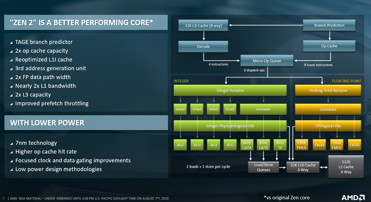
The Zen 2 blueprint underpinning Epyc 7002 Series is a known quantity because it is the same overarching architecture that powers the new breed of client Ryzens. At the front end, Zen 2 employs an L1 Perceptron and L2 TAGE branch predictor that, according to AMD, has a one-third lower misprediction rate than the Perceptron-only predictor on original Zen. So whilst this new front-end setup uses some more energy than before into reducing mispredicts, the overall net benefit is positive as the processor wastes less time in flushing incorrect branches out of the pipeline. In concert, various front-end buffers - L0 BTB, L1 BTB and L2 BTB - are made approximately twice as large to hold more branches, as is the micro-op cache, which is a handy store for already-decoded instructions.
And this is iterative processor design in a nutshell - architects take educated decisions on how and where to lay down extra transistors so that they are going to be most useful for the workloads the chip will likely handle across its lifetime.
In an interesting move, after analysing numerous applications and their dataset size, the instruction cache drops from 64KB to 32KB but increases associativity from 4-way to 8-way. The reason is that, according to Mike Clark, chief architect, this reduction barely reduces performance: most datasets need way more than 64KB anyway. The new cache features improved prefetching and better utilisation, too. What all this means is that Zen 2's front-end is more efficient - helping IPC - but does come at the cost of taking up a bit more space.
 |
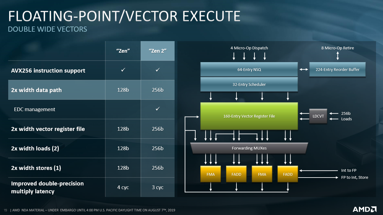 |
The move to a 7nm process is a big deal. Its density boost over 14nm/12nm gives AMD room to add more performance-enhancing transistors. Mike Clark noted that while the competition, Intel, has integrated DL Boost (AVX512) technologies to accelerate AI workloads on its newest Xeon processors, with bfloat16 floating-point support coming in the next generation, AMD felt that, for a 2019 launch frame, it would be better fit for Epyc 7002 Series to transition from AVX128 to double-wide AVX256 instruction support.
This is a literal doubling of floating-point performance over the last generation - what it took Epyc 7001 Series two cycles, or micro-ops, to do can now be accomplished in one on Epyc 7002 Series - and this is why you see AMD say there is up to 4x TFLOPS per socket - double the cores, and double the floating-point performance. Having wider registers and loads increases transistor budget, of course, yet AMD felt architecturally obliged to go down this route given how server workloads have developed in certain segments. Improving floating-point support has the ancillary benefit of also improving integer performance, as well.
To sufficiently feed the extra floating-point resource, Zen 2 also doubles the L1 read/write bandwidth to 256 bytes per cycle and, as you will know from 3rd Gen Ryzen, each four-core CCX's L3 capacity is doubled from 8MB to 16MB. What this means for the range-topping 64C/128T Epyc 7742 processor is a whopping 256MB of L3 cache. The reason for laying down so many transistors for the last-level cache is to mitigate, as much as possible, the higher latencies that arise when the processor has to spool out to main memory, which remains the same as eight-channel Epyc 7001 Series, albeit now run at a higher DDR4-3,200MHz speed.
 |
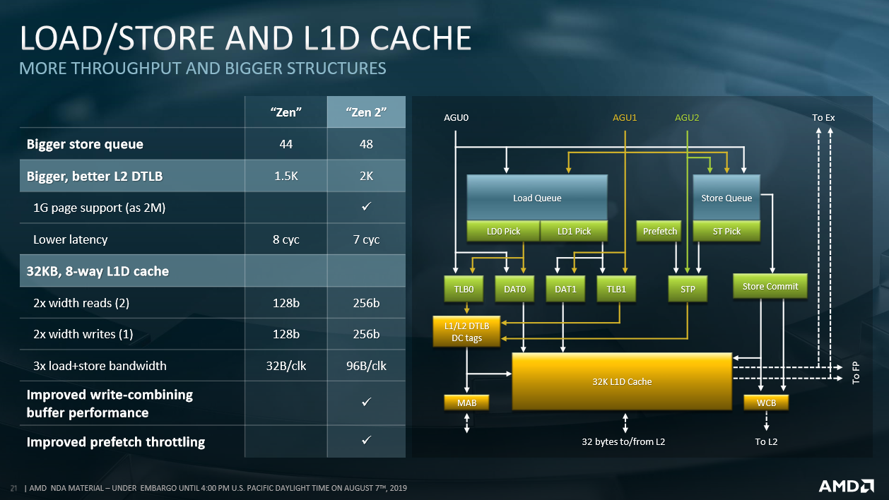 |
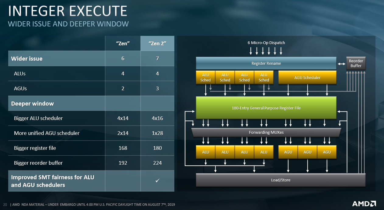
Speaking of floorplan space benefits of 7nm, particularly as it pertains to integer capability, Zen 2 includes a third address-generation unit (AGU) for accelerating the calculation of addresses needed before grabbing data from memory. Zen 2 also changes how the AGU queues are structured, going from a two 14-entry to a single 28-entry that repickers pick from. This is another case of increasing efficiency by ironing out some of the kinks present in original Epyc. The load-store bandwidth, meanwhile, is tripled because of the extra AGU and double-speed read/writes.
In summary, Zen 2 offers about 15 per cent extra IPC over Zen due to the architectural choices discussed above. The benefits of 7nm enables AMD to shoehorn twice the number of cores and, with a doubling of floating-point performance, the design has up to 4x FP capability per socket.
AMD Epyc 7002 Series SoC Implementation
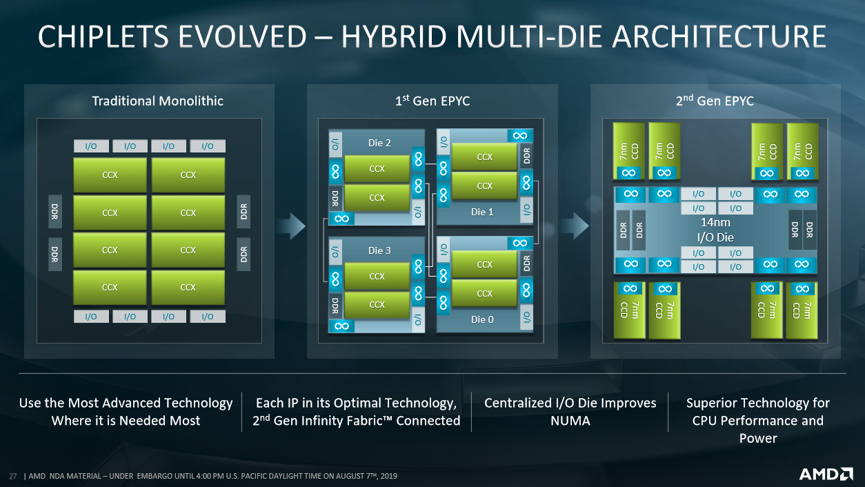
Like the desktop Ryzen counterparts, AMD splits the design into two. Leading-edge 7nm is used for the cores, as described above. According to AMD's Kevin Lepak, it doesn't make sense to use the same dense, expensive process for the I/O die because there exist a number of physical constraints that inhibit scaling effectively to lower geometries. It therefore makes sense to use a more mature, trailing process, which for Epyc 7002 Series is 14nm. Asked why AMD had used 14nm here and not 12nm present on the latest Ryzens, Kevin mentioned that they're practically the same from an implementation viewpoint.
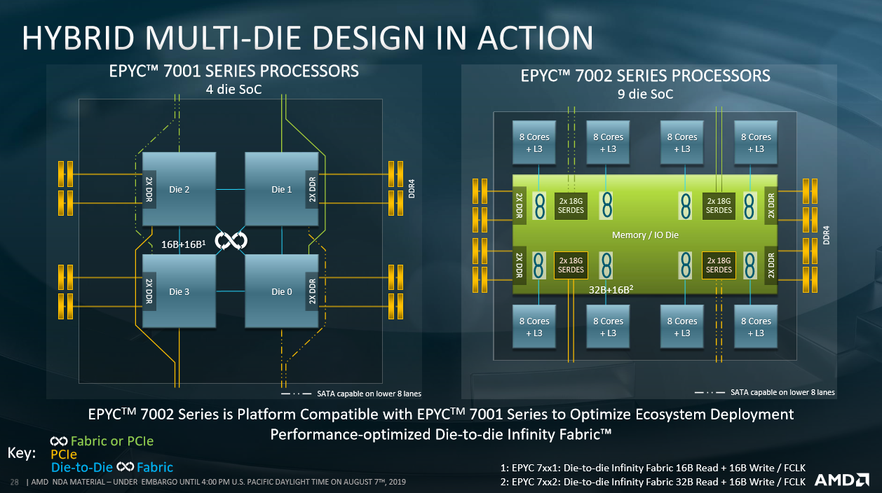
The big change, though, is how the cores are connected to the I/O die. To understand why we need to compare and contrast Epyc generation. The first topped out at 32 cores - eight per die/complex on the left-hand illustration. Each of the four dies actually holds two CCX units - in turn composed of four cores and associated L3 cache - which are connected to one another via intra-chip Infinity Fabric. Each two-CCX die has its own, individual dual-channel memory controller. Adding all this up means that a fully-populated first-gen Epyc chip has eight CCXes, those 32 cores, and an aggregate of eight-channel memory run at a maximum of DDR4-2666 with one Dimm per channel and DDR4-2400 with two Dimms per channel.
Second-gen Epyc, meanwhile, has up to eight similar dies, and keeping them connected the same way as first-gen Epyc makes little sense: one would end up with too many Numa domains, too much traversing between dies, and inconsistent memory-access latency as, for example, Die 0 pulled data from the farthest memory controller connected to, say, Die 7. Reorganising this die-to-I/O connection for greater efficiency has been critical to AMD being able to scale the processor to a higher number of cores.
Epyc 7002 Series does this by using a large centralised I/O, which is the sole conduit between the logic on the chip and pins on the package. The benefit of this approach is there is no need for data to move through other cores, which increases latency, and it positions everything literally closer together.
Providing insight, this centralised layout means that memory latency is reduced and more consistent. AMD's Kevin Lepak suggested that the variation in memory latency - a page miss, effectively - between a 2P processor configuration is 33ns lower on second-generation - 201ns vs. 234ns.
Just like the latest Ryzen, every eight-core Epyc 7002 Series die connects to the IOD/memory controller section via second-generation Infinity Fabric running at 32 bytes, per fabric clock, for read and 16 bytes for writes. This I/O section also houses the additional connectivity for the 128 PCIe 4.0 expansion lanes baked into every second-gen Epyc.
Knowing that every Epyc 7002 processor has that eight-channel DDR4 memory interface, an interesting technical discussion is how AMD physically builds lower-core Epyc processors using this distributed layout, particularly those with, say, eight or 12 cores. Having an eight-core model use just a single die makes the design highly imbalanced - there's heaps more memory bandwidth than capacity for the die to absorb it all over the Infinity Fabric link, while the ability to write at only 16 bytes a cycle, per clock, further limits what a single-die, eight-core Epyc can do. The actual implementation will reveal all.