

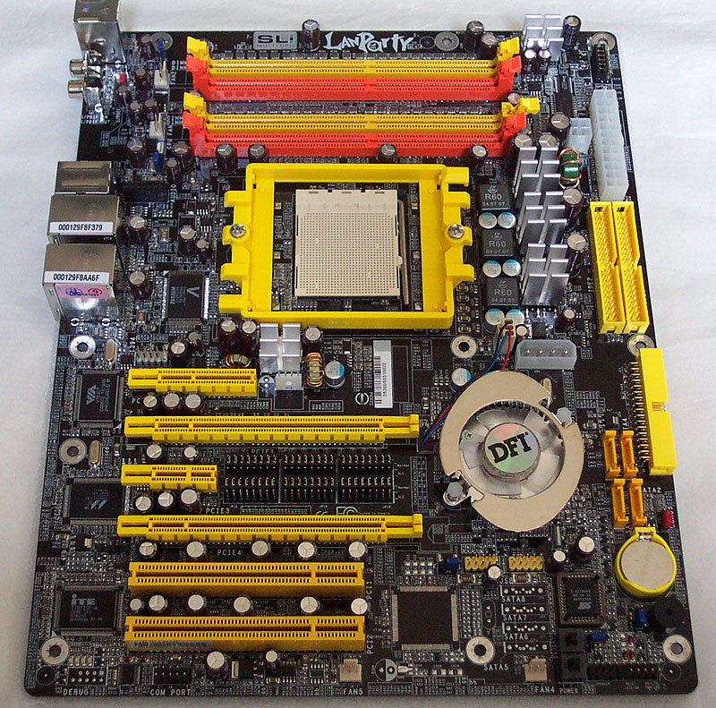
DFI LanParty UT nF4 SLI-D - Layout
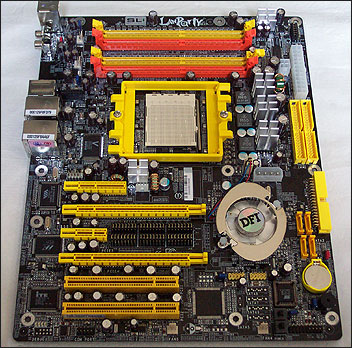
Despite sharing almost all the same features, DFI lays them out much differently compared to ASUS and the A8N-SLI. Starting at the top-left and working our way across and down, we hit a pair of fan headers first and then the memory slots, laid out horizontally across the top of the CPU socket. If you're only running two sticks of memory, DFI recommend you place them in the two orange sockets which share one channel on the memory controller.
Placing the sockets at the top of the board lets DFI route the traces back to the CPU socket area more easily, especially with the CPU oriented as it is (lever travels north-south). Traces can be shorter, improving signal integrity, especially at high frequencies. Although it's an arguable benefit at DDR400 signalling, it's logical to assume it has some effect on overclocking ability at the very least.
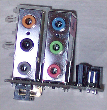
You can just about see the header for the Karajan audio pod, under the fan headers. The supplied pod contains the ALC850 chip, making it upgradable, and has the 3.5mm jacks on the assembly too. You can just snap on a new pod in the future (if any become available) to upgrade your audio CODEC and speaker support.
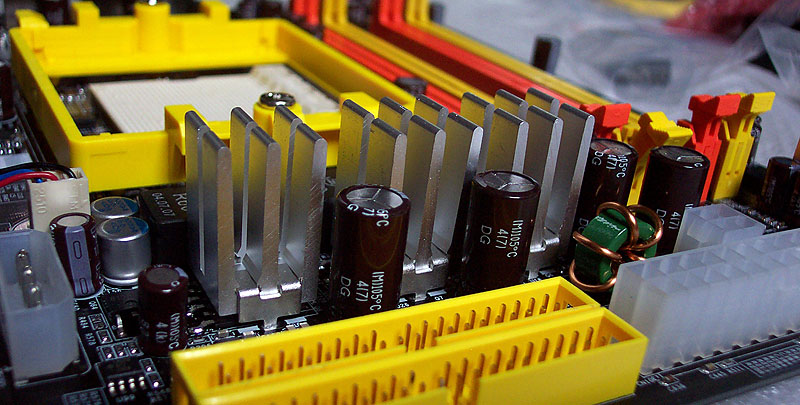
There's a heatsink for what's probably a memory voltage circuit MOSFET on the top right of the board, to keep that switching device cool, along with the jumper block to set a different range of memory voltages. With the jumper block in the default position as shipped, the BIOS will offer you 2.5V to 3.2V Vdimm. Move the jumper while the system is off and restart and you'll get 3.2V to 4.0V to play with. It's the first time such a massive range of voltages has been available from a mainboard, DFI's Oskar Wu giving a serious nod to the hardcore tweaker with that ability.
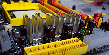
EATX main power and ATX12V (or P4 as you'll see it labelled on some PSUs) are right next to each other on the right edge of the board, near the top under the memory voltage jumper block. Placing them together like that saves you having to route ATX12V round the CPU socket area as you have to do on most boards. The CPU socket area is next, obviously shifted slightly down the mainboard compared to where you'll see it on many other mainboards, due to the memory socket placement. You can see a three-phase power delivery circuit next, the FETs cooled by heatsinks to help them operate correctly at high Vcore and CPU frequency, another large nod to the overclocker by the mainboard designer.
You can see the Vitesse Phy. chip for the NVIDIA GigE controller on the bridge, just to the left of the CPU socket. Going back to power delivery, DFI require that you assist the CPU with an extra 12V source, fed by the Molex plug just under the heatsinks on the FETs. There's also a heatsinked FET under the CPU socket area which is switching voltage for a second 12V feed you must supply, via a floppy power connector, that provides extra power to the PEG16X slots for graphics cards.
Although the DFI LANPARTY UT nF4 SLI-D mainboard will apparently still work without these two additional 5V/12V power connectors being connected, they're there to provide more stability to the entire system; as DFI go on to state that if using two high-performance 3D graphics accelerators, it's recommended that these additional 5V/12V power connectors are populated, we suggest that you use them whenever possible.
So in terms of power delivery, you've got four power connectors to hook up to a considered set of power circuitry obviously aimed at the enthusiast.
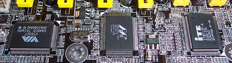
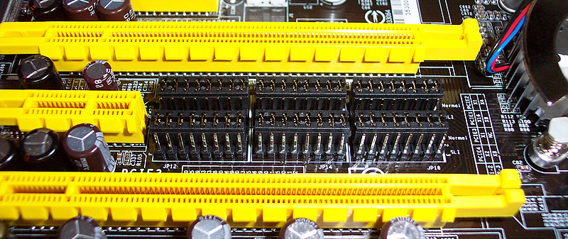
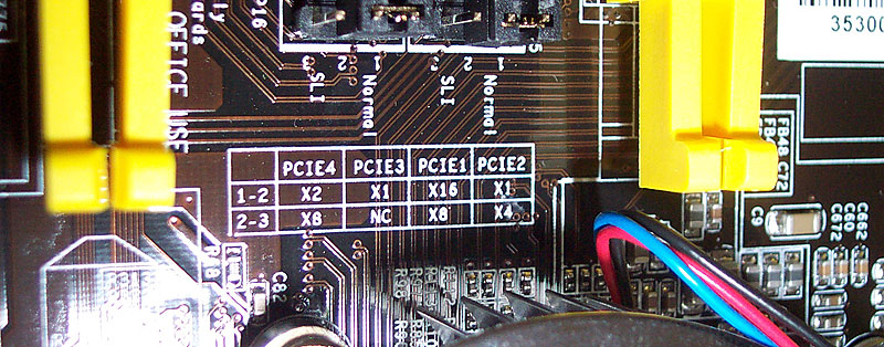
There's the main peripheral ASICs down the left hand side of the expansion slots (see those close-up, here), of which you've got a 4X PCI Express slot at the top, PEG16X, 1X PCI Express, PEG16X and two 32-bit PCI Conventional slots to fill. You can see how DFI have laid out the slots to cater for SLI and non-SLI users. In SLI mode, the middle 1X PCI Express slot is unconnected with the top slot getting its full 4X. In non-SLI mode, all four PCI Express slots get lane bundles mapped to them in a 1-16-1-2 configuration.
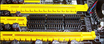
You can see the jumpers that set the operating modes, along with the table that shows you the lane assignments, in between the PEG16X slots. It's different to the continuity connector on the ASUS and other boards, and in my opinion it's a more reliable mechanism in terms of making a solid set of connections. Anyone else with an ASUS or similar will know what i mean, with the continuity connector never quite sitting in its socket solidly, feeling a little loose on all the A8Ns have had the chance to use.
To switch modes, move all the jumper blocks up or down a jumper bank. Simple stuff.
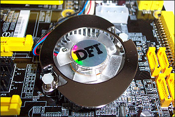
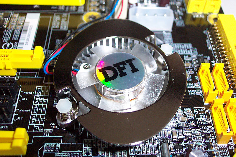
DFI place the cooler so that the fan is partly obscured by longer graphics cards you might place in the topmost PEG16X slot. That positioning, hindering cooling slightly, along with the fan itself being rather noisy and the pitch changes it makes as it speeds up and down being audible, are the bad points on an otherwise excellent mainboard. In the couple of weeks I've run the SLI-D since it arrived, the fan has made me shout (seriously) at mainboard more than once, as I struggle to find some settings in the BIOS to tame it. More on that shortly.
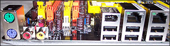
DFI lay the PATA ports vertically, just over half way up the board's right-hand edge, with the floppy port set with its face outwards. I'd liked to have seen that on the outermost PATA port too, but it's a minor point. SATA ports get oriented vertically and are pushed close to the board edge (at last!), in almost the perfect placing for them. CMOS battery sits underneath.
You can see the PCB space for the Sil3114 controller you'll get on the SLI-DR version of the board, and the space for the associated SATA ports sit next to the BIOS chip, near the USB pin headers for connecting the extra USB ports.
The last things to spot are the pair of fan headers on the bottom edge of the board giving five in total and four usable by you (one drives the nForce4 bridge's fan), and the board-mounted power and reset buttons, which DFI call EZ Touch buttons. A quick stab of them gets the board going without the assistance of a switch on a case.
Overall
Layout wise, it's fairly inspired. The only issue I had, during a system build of the DFI into my favourite chassis, was the routing of a power cable to the floppy connector that gives the PEG slots extra power.One final thing I've noticed is that the memory module closest to the CPU gets a lot warmer (10°C or more) than any above it, due to the CPU's heatsink dumping heat to the module. The fan noise gets on my nerves at times, but tweaking of its settings in the BIOS will usually sort that out for you, and it's really the only low point of a great layout and board hardware to appease the enthusiast in a big way.