

Layout and BIOS

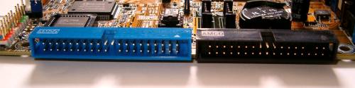
Top to bottom, left to right, as always, as you look at that picture. Power regulation hardware sits to the left of the CPU socket, itself well bounded by the regulation retention bracket that Intel specify as mandatory for all P4 board designs. There's a north-south socket orientation for the P4 socket, an optimal design choice for trace routing to the northbridge; you sometimes see an east-west layout on Canterwood boards. A small gap past the east side of the socket retention bracket and then we hit the DIMM slots. Colour coded to show you what slots fill what memory controller, the slots are laid out in a 2x2 grouping, north-south as always with a DDR P4 motherboard.
ATX power sits at the very top right of the board, a position that I'm a fan of, especially when dealing with snake-like power supplies from the likes of Enermax. The SiS964-provided ATA ports sit right underneath, another excellent place for them in modern ATX cases. In the current age of SATA, having your regular ATA ports up near the top of the motherboard, to serve optical devices that are likely to sit high up in your case, is a good design choice. Thumbs up for that.
The 655TX bridge is passively cooled by the same large, multi-fin aluminium cooler that ASUS have used on other recent motherboards like A7N8X. It's not the most stylish heatsink you'll ever see, but it is silent. No fan means no noise, something we can all be thankful for.
From there on down we're in standard layout country. 5 PCI slots means the opportunity for the AGP slot to move a slot down on your case backplane, moving it away from the bottom edge of the memory modules and avoiding collisions between your AGP card and memory modules. ASUS take that opportunity, well done to them for that.
The Marvell networking ASIC sits to the left of the PCI slots and the SiS964 bridge sits in the middle of the empty board area on the right. Everything else hangs around there too. SATA ports are either clustered when SiS964 provided, up near the battery and floppy drive port, or either side of the SiS180 when they're provided by that bit of silicon. I'm not really a fan of that kind of layout; I much prefer them clustered together for cable routing reasons, but it's not too bad. At least they aren't too far away from the right edge of the board, the best place for them.
The FireWire400 controller is near PCI3 and PCI4, the SiS180-provided ATA port is rotated out towards the board edge, a brilliant design choice for those type of ports. My only grumble is that they don't do it with the port nearest the board edge at the top as well.
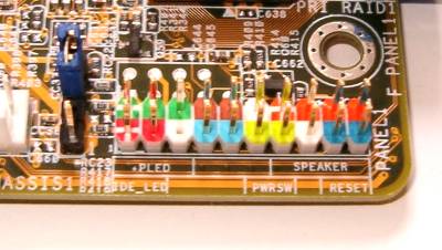
Coloured ATX case header pins, clearly labelled too, are the final board highlight. Everyone should do it, thumbs up for ASUS for putting it in to practice.
BIOS
I'll hold my hands up here, I realised I'd forgotten to take BIOS shots for the P4S800D-E after it had gone back to ASUS. Being a brand new board, I only had a few days with it before ASUS had it whisked off to some other site for review. So no BIOS photos or CPU-Z work in this review, I'll move that item near the top of my to-do list in future.The BIOS itself was an AMI-style implementation with the usual animated scrolling top bar that you'll see on all recent ASUS BIOS implementations. Being SiS655TX-based, the BIOS for P4S800D-E Deluxe had an obvious 655TX slant, to complement the usual adjustment of things like date, time and ATA settings. As far as the memory controller settings went, you can force the 64-bit x 2 mode if you really want to, even with matched DIMMs, and you get the usual adjust over CL, Tras, Trcd and Trp.
With an unlocked ES processor you get multiplier adjustment, the usual 12x to 16x were all correct choices on the HEXUS test 3.2ES. Hardware monitoring was notable in its flexibility; it shares the same selective choices over what you want to monitor with recent K8V BIOSs available for that particular board. After that things are pretty standard. You can turn on and off the USB ports, the FireWire controller, the AD1988 CODEC and things like the serial ports.
Overclocking wise, you get front side bus adjustment (more on that later) and limited voltage adjustment. The BIOS only seemed to allow 0.1V+ CPU boot Vcore. 1.625V was the maximum recorded voltage in the BIOS when setting it, so at least it was spot on.
Again, apologies for no specific BIOS photographs in this review. The BIOS was a lot more interesting than you usually see, due to the chipset of choice. Damn me!
System setup next before we move on to pretty graphs and a look at performance.