More than meets the eye
The consumer solid-state drive (SSD) market has been characterised as a race to the pricing bottom, as manufacturers outdo one another by reducing margins and betting on the price of NAND flash. Such bets can realistically be taken on by those SSD guys who manufacture their own memory; doing so otherwise is fraught with danger.
But not all SSDs are created equal. Newer interfaces such as M.2 and PCIe remove some of the limitations inherent in SATA 6Gbps, notably sequential bandwidth, though many SSDs - composed of controller and NAND flash - are now engineered to meet a specific purpose. Consumer SSDs promulgate sequential speed and low cost, while enterprise drives focus on reliability, quality of service and performance consistency.
Supplementing entry-level enterprise
It's to enterprise SSDs that we turn to in this review. Samsung released the 845DC EVO trio of entry-level enterprise drives early last month. Available in 240GB, 480GB and 960GB capacities and using the latest 19nm Toggle Mode NAND, though reducing costs by implementing 3-bit-per-cell TLC memory instead of commonly-used 2-bit-per-cell MLC, Samsung is now following the EVO range up with a couple of PRO models.
Perhaps the 400GB and 800GB 845DC PRO are needed because enterprise customers still don't have complete faith in using TLC NAND for mission-critical applications. Going back to MLC NAND and adding a very healthy amount of overprovisioning - where user-inaccesible capacity is set aside for better wear levelling and buffering - enhances endurance. Let's dig deeper with a look at a comparison table.
Samsung SSD 845DC Series |
|||||||
|---|---|---|---|---|---|---|---|
| Family | 845DC PRO |
845DC EVO |
|||||
| Model | 400GB |
800GB |
240GB |
480GB |
960GB |
||
| Processor | Samsung 3-core MEX |
||||||
| NAND | Samsung Toggle 2bit 3D V-NAND (MLC) |
19nm Samsung Toggle 3bit NAND (TLC) |
|||||
| Total Drive Capacity | 400GB |
800GB |
256GB |
512GB |
1,024GB |
||
| Onboard DDR2 Cache | 512MB |
1GB |
512MB |
512MB |
1GB |
||
| Interface | SATA 6Gb/s, compatible with SATA 3Gb/s and 1.5Gb/s |
||||||
| Sequential Read Speed | up to 530 MB/s |
up to 530 MB/s |
up to 530 MB/s |
up to 530 MB/s |
up to 530 MB/s |
||
| Sequential Write Speed | up to 460 MB/s |
up to 460 MB/s |
up to 270 MB/s |
up to 410 MB/s |
up to 410 MB/s |
||
| Random IOPs (4KB Reads, QD32) | up to 92,000 IOPs |
up to 92,000 IOPs |
up to 87,000 IOPs |
up to 87,000 IOPs |
up to 87,000 IOPs |
||
| Random IOPs (4KB Writes, QD32) | up to 50,000 IOPs |
up to 51,000 IOPs |
up to 12,000 IOPs |
up to 14,000 IOPs |
up to 14,000 IOPs |
||
| Quality Of Service (4KB, QD32) | 99.9% Read: 0.6ms, Write 7ms Max. Read 3ms, Write 12ms |
99.9% Read: 0.6ms, Write 7ms Max. Read 3ms, Write 8ms |
|||||
| Latency (4KB, QD32) | Sequential: Read 45us, Write 40us Random Read 110us, Write 50us |
Sequential: Read 55us, Write 45us Random Read 115us, Write 55us |
|||||
| Dimensions (LxWxH) | 100 x 69.85 x 6.8 (mm) |
||||||
| Active Power Consumption | Read/Write 1.7W/3.1W |
Read/Write 2.7W/3.8W |
|||||
| Idle Power Consumption | 1.0W |
1.2W |
|||||
| Life Expectancy | 2 million hours Mean Time Between Failures (MTBF) |
||||||
| Endurance | 10 Drive Writes Per Day |
Up to 600TB TBW (960GB) |
|||||
| Warranty | 5 Years |
||||||
3D comes to NAND
Samsung introduces what it terms 3D V-NAND for these new PRO models. This is a cell layer-stacking technology where 24 layers are built up on a single NAND, rising to 32 for the next generation of SSDs. Do be aware that cells are stacked, not chips. V-NAND, in general, based on larger processes, helps mitigate problems of reduced endurance and poorer performance when NAND is scaled down to 1xnm.
There's more. Flash memory uses an electrically-isolated floating gate underneath the control gate - CPU transistors only have a single gate - and its purpose is to increase the voltage threshold needed for the transistor to become conductive. When charge is put through the control gate to the floating gate, the memory is said to be programmed. Removing the charge erases the contents.
Samsung says that instead of using the traditional floating gate to add or remove charge coming from the control gate, which is extremely difficult to do when building for a 3D device, it is supplanting it with a charge trap, which is a non-conductive layer that effectively wraps around the transistor. This layer has lower-leakage properties, requires less voltage to function and therefore uses less energy. A by-product of lower voltage is less stress and increased endurance than would be possible by using a traditional floating gate.
Also, moving to a 3D cell-stacking model means that compared to regular 'flat' planar NAND Samsung's 3D V-NAND requires less physical space for the same capacity - multiple cell layers are stacked on top of each other, remember - thus removing the need to run with ever-smaller process geometries.
Better endurance, improved quality QoS
The 845DC PRO's NAND uses the 24-layer version of this 3D-stacking technology. Notice that write endurance is listed as 10 drive writes per day. This, for the 800GB model, leads to a 14,600TB Total Bytes Written (TBW) over the five-year warranty period, compared with 600TB for the standard 845DC EVO and most similar enterprise SSDs. Why is this possible? On top of the benefits of a lower voltage for the charge trap, having to go to smaller process geometries hurts SSD endurance, so the ability to run larger-geometry flash certainly helps in this instance.
A couple of other advantages are apparent from Samsung's approach. Larger-geometry NAND enables faster programming (more speed) as does the use of charge-trap technology over traditional floating gate. Putting the two together should lead to improved overall performance.
Enterprise SSDs also need to exhibit consistent performance once a steady state has been reached. Just like the 845DC EVO, the PRO executes 999 out of 1,000 read requests within 0.6ms, and write requests within 7ms. IOPs consistency can also be measured another way, by calculating how close the worst 0.1 per cent IOPs is to the average. Samsung reckons that in this case the worst 0.1 per cent is at least as 90 per cent as good as the average for reads and 95 per cent as good for writes.
Bottom line is that the worst-case performance is very close to the average. Low latency and high Quality of Service are prerequisites for a good datacentre drive. Sequential numbers are decent, too, with hugely-improved IOPs for 4K writes at a queue depth of 32. Why? this is most likely due to the aforementioned use of a larger-geometry NAND and charge-trap technology.
The drive
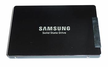
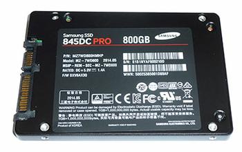
Encased in a 7mm-high package and similar in look and feel to almost all other Samsung SSDs, the 845DC PRO uses the same metal construction and perfunctory design.
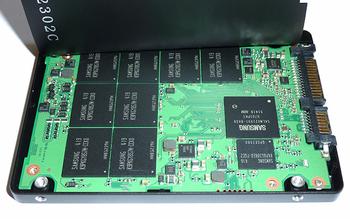
Gaining access to the drive requires removing three mini-Torx screws. This non-standard approach has the benefit of reducing returns, we guess, as finding the right tool for the job isn't easy. Compounding matters, one of the screws - bottom-right - became rounded at the lightest of touches.
But we can still take a peek at what's inside. The three-core MEX controller remains the brains of the outfit, and just as with the 845DC EVO, it's clocked in at 400MHz, or 100MHz higher than the 840 PRO consumer drive you're likely familiar with. Backing the controller is, for this model, 1GB of DDR2 cache. Samsung also invests in tantalum capacitors, whose job it is to protect the data in the write cache should power be lost to the unit.
This first-generation 3D V-NAND is known as K9PKGY8S7M-CCK0. Eight 128GB chips constitute a nominal 1,024GB capacity. Samsung is keeping heck of a lot of spare capacity back for overprovisioning purposes, further reinforcing the endurance-focussed nature of the drive.
Summary
Samsung is using a combination of extensive overprovisioning and new 3D V-NAND technology to improve the endurance, speed and consistency of the 845DC PRO when compared to regular drives using planar cells based on small-geometry flash. Let's now find out how fast and consistent this new drive is.


