A team of researchers from MIT and the University of Chicago have devised a technique for creating patterns of lines and wires much thinner than is possible using traditional micmrochip fabrication methods. Importantly, the new microchip self assembly process can use existing lithographic machinery and the underlying chemical process is well understood. What this means is that implementing the new method to make much finer micro circuits could be attractive to chipmakers.
Professor Karen Gleason at MIT explains the problem facing the semiconductor industry; "People always want smaller and smaller patterns, but achieving that has been getting more and more expensive." So how can the researchers create finer patterns and lines with existing fabrication equipment? It is explained as a three step process, using the lithography machines available now and well understood polymer chemical processes.
- First a pattern of lines is produced on the chip subscrate using well established lithographic techniques
- Secondly, a block copolymer layer is laid down. Made of chain-like molecules of two different polymer materials the layer will predictably segregate itself but remain bonded (this is the beginning of the 'self assembly' stage).
- The third step is the adding of a top protective polymer using initiated chemical vapour deposition (iCVD). The top layer constrains the self-assembly of the co-polymers below so they are forced into vertical layers. MIT News describes the layers as resembling a layer cake on its side; I'm thinking 'Signal' toothpaste.
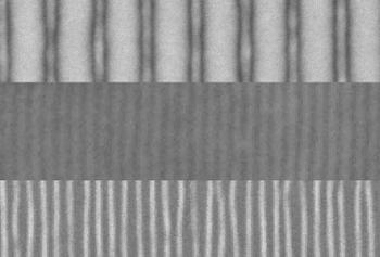
During the above processes the polymers follow the underlying guides but their natural properties cause their widths to be much reduced and there can be four or more lines in the place of one underlying lithographic line. The process can use simple lines or complex patterns to build upon various lithographic circuit features.
These scanning electron microscope images show the sequence of fabrication of fine lines by the team's new method. First, an array of lines is produced by a conventional electron beam process (top). The addition of a block copolymer material and a topcoat result in a quadrupling of the number of lines (centre). Then the topcoat is etched away, leaving the new pattern of fine lines exposed (bottom). Credit: MIT News.
According to an independent chemical engineering professor, Joerg Lahann, at the University of Michigan, the above research provides "major progress in the area of nanofabrication," at sub-10nm. "The fact that they can demonstrate arbitrary structures highlights the quality and versatility of this novel technology," added Lahann.


