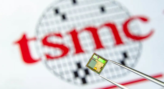
An important paper on semiconductor technology penned by research scientists from Taiwan Semiconductor Manufacturing Company (TSMC), the National University of Taiwan (NTU), and Massachusetts Institute of Technology (MIT) has been published by Nature (spotted via Verdict). The tripartite have announced a breakthrough in the use of 'beyond-silicon' and 2D materials in electronics. The research provides a path to electronics manufacturing processes of 1nm and lower, helping break past the limits of current semiconductor tech and materials.
Scientists have for a long time looked towards the potential of atomically thin two-dimensional semiconductors in realising high-performance electronic devices. However, there have been two significant problems to migrating semiconductor production to use this new tech. Firstly the materials had an inherent property of high contact resistance, and secondly they had poor current delivery capabilities. Now TSMC, NTU, and MIT appear to have solved these issues.
According to the research paper, the scientists have cracked the above-mentioned problems and achieved "zero Schottky barrier height, a contact resistance of 123 ohm micrometres and an on-state current density of 1,135 microamps per micrometre on monolayer MoS2". These are said to be the best values ever for these materials, and hold promise for extending Moore's Law.
It is interesting to read how the tripartite worked together over 18 months to make these advancements. Apparently MIT made the key discoveries behind the new technology, then TSMC's expertise allowed it to be optimised via an "easy deposition process", last but not least NTU stepped up to leverage its helium ion beam lithography to narrow the component channel to 1nm.
A fortnight ago IBM unveiled its breakthrough 2nm nanosheet chip technology, and as a close Intel partner we should expect this tech to be used in making processors in a few years time, probably the latter half of the decade. The latest manufacturing news we had from TSMC meanwhile, is that its 5nm production capacity is going to double this year, 4nm is running ahead of schedule, and it already finished construction of its first 3nm factory last November (with mass production scheduled for H2 2022).