AMD Zen 2 and Zen 3 processor 7nm preparation has been tough

by Mark Tyson on 25 July 2017, 11:01

Tags: AMD (NYSE:AMD)

Quick Link: HEXUS.net/qadjw5

Add to My Vault: x

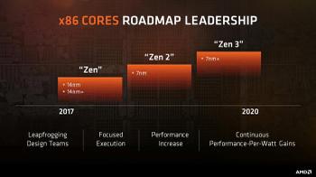
AMD CTO Mark Papermaster has been discussing the company's plans, in a wide ranging interview with the EE Times. In the chat Papermaster confirmed that both AMD Zen 2 and Zen 3 processors will be made in 7nm and that he would like foundries to introduce EUV "as fast as they can". AMD has been making good progress with its preparation for 7nm, said Papermaster, but it's such a big change that both foundry and design teams have had to double their efforts.

Moving to 7nm is the "toughest lift I’ve seen in a number of generations," admitted Papermaster in the interview. There are a number of reasons behind the difficulties, but two major ones cited are; the requirement for new CAD tools for 7nm, and the need for deeper cooperation with foundries and the EDA (Electronic Design Automation) industry. Going forward there will of course be difficulty for the foundries in producing the AMD chips on new 7nm processes.

Discussing the design process Papermaster told the EEtimes that 7nm is "a long node, like 28nm…and when you have a long node it lets the design team focus on micro-architecture and systems solutions," rather than redesign standard blocks for the next process.

The CPUs and GPU currently shipping are among the first designs in 14/16nm nodes using double patterning lithography and FinFET transistors. EUV processes, which will reduce the need for quad patterning and have the potential to lower costs and shorten design cycles, should be live in 2019, thinks Papermaster.

AMD has been working with Globalfoundries for CPUs and TSMC for GPUs and Papermaster has been happy with this choice. Furthermore both companies have "been aggressive in 7nm and that’s good for the industry" he said. Intel doesn't have any advantage in process tech due to this strong competition. However the AMD CTO urged foundries to move as fast as they can to keep up competitive pressure.

Later in the interview Papermaster went on to discuss 2.5D chip stacks. This tech is great for high end graphics processors, for example, but is flagged as being too expensive. In the meantime a so-called 2.1D technology could work out well, but it will take 2 or 3 years to be ready for AMD's desktop and server processors.


HEXUS Forums :: 11 Comments

Login with Forum Account

Don't have an account? Register today!
I don't know why but I am really excited for the 7nm node, it will be a big jump for both companies and because it's a completely different scale it will be interesting to see how both companies fight on a level playing field.
Tabbykatze
I don't know why but I am really excited for the 7nm node, it will be a big jump for both companies and because it's a completely different scale it will be interesting to see how both companies fight on a level playing field.

By ‘both companies’, do you mean Intel & AMD? Because they're effectively on a level playing field now - they're both at 14nm…
MrJim
By ‘both companies’, do you mean Intel & AMD? Because they're effectively on a level playing field now - they're both at 14nm…

Well its more the case Samsung 14NM was a process more orientated towards mobile and is basically 20NM with finfets.

7NM should be realistically closer to Intel 10NM,and is a high performance process which had IBM involvement.

OFC,we will need to wait and see,but it MIGHT mean they get closer together in clockspeeds.
Can anyone reasonably guess the kind of increase in perf/watt we'll likely see?
MrJim
By ‘both companies’, do you mean Intel & AMD? Because they're effectively on a level playing field now - they're both at 14nm…

Yes, but AMD was late to the 14nm party so Intel had the home advantage whereas if they both arrive onto the node together we will see genuine competition where time and experience with the node will put you ahead.

chj
Can anyone reasonably guess the kind of increase in perf/watt we'll likely see?

https://www.globalfoundries.com/technology-solutions/cmos/performance/7nm-finfet

This technology provides world-class performance, power, area and cost advantages from 7nm scaling. Based on 3D FinFET transistor architecture and optical lithography with EUV compatibility at key levels, 7LP technology delivers more than twice the logic and SRAM density, >40% performance boost and >60% total power reduction compared to 14nm foundry FinFET offerings.