The Taiwan Semiconductor Manufacturing Company (TSMC) virtual Annual Technology Symposium is currently taking place. It seems like the contract semiconductor manufacturer is going from strength to strength right now, and the symposium presentations make it look like this good fortune is set to continue for the foreseeable future.
Last week HEXUS wrote about TSMC's massive milestone in N7 (7nm) chip production - that it had manufactured "one billion functional, defect-free 7nm chips" since April 2018. The process is used by many PC component makers in CPUs, GPUs, 5G and networking chips, and more - 140 designs currently use N7 and that number is expected to rise to 200 by the end of the year.
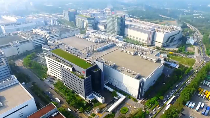
Coming up shortly will be the proliferation of products built on N5. TSMC started volume manufacturing of N5 in Q2 this year. Apple's next A-Series processors are expected to be amongst the first components to benefit from this cutting edge process. We will hear about these pretty soon when the next gen iPhones are announced, and we might at that time learn more about new iPads, and the exciting new range of Mac computers powered by 'Apple Silicon'.
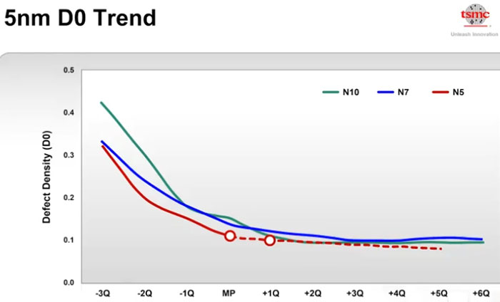
On the topic of N5 this process is said to be progressing with defect densities a quarter ahead on N7, which is a good sign. According to TSMC N5 will be 15 per cent faster, 30 per cent lower power, with a 1.8X density versus N7. N5P will finesse things further by adding an extra 5 per cent speed and reducing power consumption by 10 per cent.
N4 will be an extension of N5 and thus offer a straightforward migration path for N5 users/products. TSMC says it will start N4 risk production in Q4 2021 with volume production estimated to begin in 2022.
N3 is FinFET based with full 3nm scaling in effect. It will enter risk production in 2021 with volume production to follow in H2 2022. TSMC has some perf/power projections for N3 vs N5 (not N5P). N3 will deliver a 10 to 15 per cent performance increase, with 25 to 30 per cent reduction in power, with a 1.7x logic density, and 1.2x SRAM density, and 1.1x analogue density.
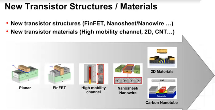
How to progress beyond 3nm?
TSMC 3DFabric
TSMC isn't just following the tried and trusted process shrinking path, it has some other technologies at play to keep ahead of the pack. At the symposium TSMC announced its 3DFabric technology which represents a set of advanced packaging techniques for chip stacking (chip-on-wafer, wafer-on-wafer) and advanced stacking of chips, interconnects, interposers, memory, and so on.
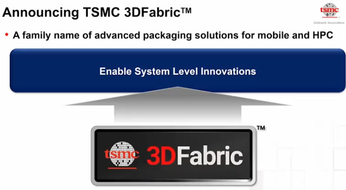
These advanced 3D packaging technologies will help partners build feature rich SoCs with reduced form factors, improved bandwidth, and with lower power consumption and should work great in concert with the node scaling via refined process technologies.
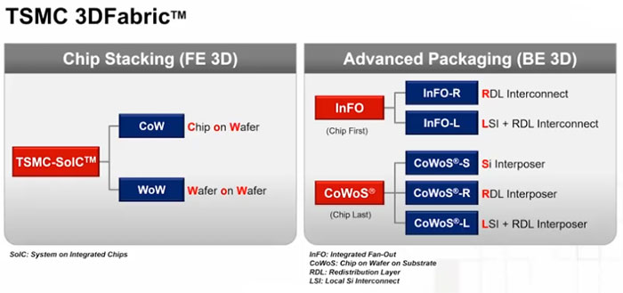
At the time of writing the TSMC virtual annual Technology Symposium materials are yet to be published online in the usual places, so I had to grab screens from the live presentations. I think TSMC press releases and blog posts will be up for further reference later this week.
Other sources: Patrick Moorhead, Andandtech.


