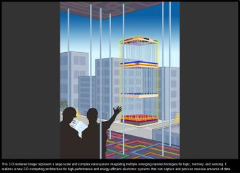
A new type of computer chip, built to tackle huge amounts of data, has been designed by researchers at Stanford University and MIT. It aims to revolutionise computing by combining breakthrough nanotechnologies in an innovative 3D structure.
A great deal of time and energy is wasted in computer systems, shuttling data back and forth between storage to processing. Furthermore, Silicon is reaching the limits of its scope to be miniaturised. Thus the scientists at Stanford University and MIT have been testing a new prototype chip with an innovative computer architecture to address both the aforementioned concerns.
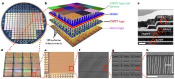
The prototype combines 2 million carbon nanotube field-effect transistors and over 1 million RRAM nonvolatile memory cells into "the most complex nanoelectronic system ever made with emerging nanotechnologies," reports the MIT News Blog.
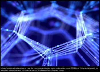
It is explained by the blog that "The RRAM and carbon nanotubes are built vertically over one another, making a new, dense 3-D computer architecture with interleaving layers of logic and memory. By inserting ultradense wires between these layers, this 3-D architecture promises to address the communication bottleneck." Such an architecture would not be possible with existing silicon-based technology, asserts the lead author of the research paper, Max Shulaker.
Interestingly one of the key benefits of fabricating the new computer chips stems from the much lower temperatures involved in fabrication. Silicon chip creation requires temperatures up to 1,000 degrees Celcius, so it's difficult to make multi-layers and 3D structures without damaging prior layers. However "carbon nanotube circuits and RRAM memory can be fabricated at much lower temperatures, below 200°C", says Shulaker.
The result is that Stanford University and MIT's prototype chip and its 3D architecture will be able to be made denser, more efficient, and without the associated bottlenecks in todays silicon-based computer systems. Despite the differences, professor Roger Howe from Stanford says that the chip that was demonstrated "is compatible with today’s silicon infrastructure, both in terms of fabrication and design".


