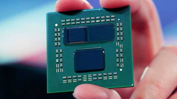
Back at the start of Computex 2021, AMD's keynote was pretty packed with juicy details about its Ryzen processors and Radeon GPUs, as well as news of the impending launch of FidelityFX Super Resolution (FSR), and a closer look at upcoming 'Advanced Technology'. A specific advanced technology catching hearts and minds from the showcase was AMD's 3D chiplet technology using 3D stacking, and a prototype modified Ryzen 9 5900X which had 3D stacking implemented by including a 3D V-Cache.
In the above linked article, I talked about the new packaging tech being applied to caching and included slides illustrating its application and potential benefits in gaming. Going forward AMD will be using the same tech for other stacking purposes, but it seems to have chosen the cache as the first target for the instant obvious benefits it could deliver – with fast cache so much closer to the processing.
AMD must think its "revolutionary 3D chiplets" need some further explanation / highlighting, as it has now published one of its regular 'The Bring Up' technology chat videos on its official YouTube channel. We got some extra insight into the process of creating these 3D V-cache processors, and plenty of chat about its importance too. See below.
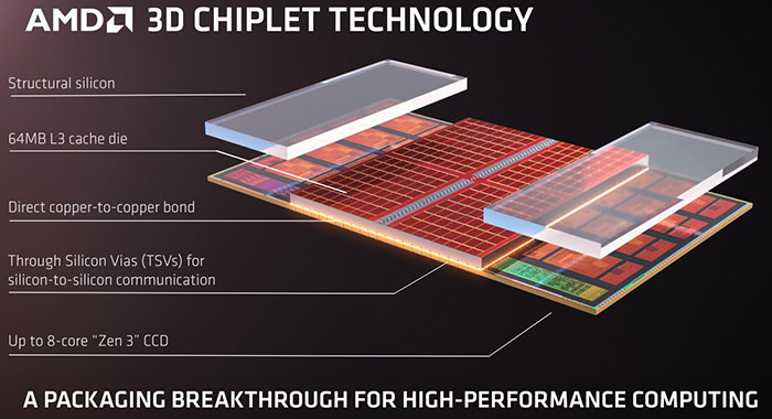
Above it is revealed that before the cache silicon is put on top of the CPU dies it is shaved to just 20 micrometers thick. Thus, the cache and core physical distance in the new architecture is cut by a factor of a thousand compared to the previous side-by-side architecture. The greatly reduced distances, for the electrical signals to travel, means faster signalling, plus reduced heat and noise generation potential in the chip design.
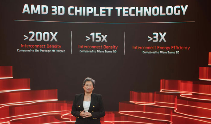
It was explained by the presenters that, previously, chips were put together using the 'Controlled Collapse Chip Connection' (C4) process with solder balls connecting processor to board. The new 3D chips utilise copper bonding by Through Silicon Vias, or TSVs (with the dies shaved so thin for very short TSVs) which are easy to pack much more densely than solder balls. In the same area you can get many more paths for signals (>200X density compared to 2D packaging, >15X interconnect density compared to micro bump 3D) and more evenly distributed power too.
In the video you will see Cavin and Bridget demonstrate the benefits of a 1000x factor reduction in electrical transfer distance – but on the macro scale – showing the signal delays, or latency in the comparison. On the nano-scale used by today's chipmakers differences in distance are much smaller of course, but with chips transferring data billions of times per second the savings add up.
Bake cookies or get Control for the weekend
A less useful visual metaphor regarding chip densities was provided by a light-hearted chocolate chip cookie making skit towards the end of the video, which I encourage you to skip. Instead, use the time to go and download a copy of Control, free until 17th June, from the Epic Games Store.