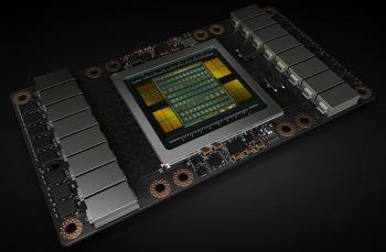
A few hours ago at the GTC 2017 Nvidia CEO Jensen Huang took the wraps off the Tesla V100 accelerator. This launch marks several milestones for Nvidia, not least the introduction of its first Volta architecture GPU based product. As those familiar with Nvidia's nomenclature will be aware, the first product based upon Volta is an accelerator targeting complex problem solving. The Nvidia Tesla V100 is referred to in headline terms as an "AI computing and HPC powerhouse".
Following hot on the heels of its Q1 financials, showing stellar performance in its datacentre business, Nvidia looks to be keeping the pressure up on this sector. Furthermore, it hasn't been afraid to invest, spending $3 billion in R&D in developing Volta.
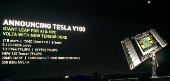
The new Volta-based Nvidia Tesla V100 packs a significantly weightier punch than the Pascal-based Tesla P100 and for the first time Nvidia has started making performance comparisons using Peak Tensor Core TFLOP/s (I'm not sure if this measurement is analogous to TOPS as used by Google in describing its Tensor Processing Unit performance).
Peak computation rates (based on GPU Boost clock rate) are:
- 7.5 TFLOP/s of double precision floating-point (FP64) performance;
- 15 TFLOP/s of single precision (FP32) performance;
- 120 Tensor TFLOP/s of mixed-precision matrix-multiply-and-accumulate.
It's interesting to see that Nvidia's Volta GV100 architecture offers dedicated Tensor Cores to compete with accelerators from the likes of Google. There are 8 Tensor Core per SM unit in the Volta GV100, that's 640 in total. They provide a significant performance uplift in training neural networks. "Tesla V100’s Tensor Cores deliver up to 120 Tensor TFLOPS for training and inference applications," notes Nvidia. I think that means the GV100 leapfrogs Google's TPU ASIC which is capable of 90 TOPS.
The Volta GV100 GPU powering Nvidia's latest accelerator product has some mighty specs. First of all, from the article subheading, you will already be aware that this GPU packs in 21.1 billion transistors and is fabricated using TSMCs 12nm FFN process. Chip size is considerably higher than the last gen, with the GPU measuring 815mm2 compared to the P100's 610 mm². Among the computing components inside a full GV100 GPU are; 84 SMs, a total of 5376 FP32 cores, 5376 INT32 cores, 2688 FP64 cores, 672 Tensor Cores, and 336 texture units. In the Tesla V100 80 SMs are enabled, so there's 5120 CUDA cores at work, probably reduced from the maximum possible for better yields and to provide room for next generation Titan headlines.
Supporting the Volta chip in the Tesla V100, Nvidia has architected an SMX card with second gen NV-Link high speed interconnect technology for up to 300GB/s links, 16GB of HBM2 memory from Samsung providing 1.5x delivered memory bandwidth versus Pascal GP100, Maximum Performance and Maximum Efficiency Modes are present, and that all-important optimised software support with GPU accelerated libraries is available.
Nvidia has published quite a lengthy blog post about the arrival of Volta with the Tesla V100 accelerator. You can head on over there to read more about the technicalities and architectural nuances of the new architecture: Inside Volta.
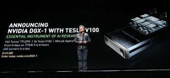
Those interested in deploying Volta based solutions should know that the first server and deep learning products based upon Tesla V100 will become available starting from Q3 2017. A DGX-1 system powered by the new GPUs will set you back $149,000 for example.
|
Tesla Product |
Tesla K40 |
Tesla M40 |
Tesla P100 |
Tesla V100 |
|
GPU |
GK110 (Kepler) |
GM200 (Maxwell) |
GP100 (Pascal) |
GV100 (Volta) |
|
SMs |
15 |
24 |
56 |
80 |
|
TPCs |
15 |
24 |
28 |
40 |
|
FP32 Cores / SM |
192 |
128 |
64 |
64 |
|
FP32 Cores / GPU |
2880 |
3072 |
3584 |
5120 |
|
FP64 Cores / SM |
64 |
4 |
32 |
32 |
|
FP64 Cores / GPU |
960 |
96 |
1792 |
2560 |
|
Tensor Cores / SM |
NA |
NA |
NA |
8 |
|
Tensor Cores / GPU |
NA |
NA |
NA |
640 |
|
GPU Boost Clock |
810/875 MHz |
1114 MHz |
1480 MHz |
1455 MHz |
|
Peak FP32 TFLOP/s* |
5.04 |
6.8 |
10.6 |
15 |
|
Peak FP64 TFLOP/s* |
1.68 |
2.1 |
5.3 |
7.5 |
|
Peak Tensor Core TFLOP/s* |
NA |
NA |
NA |
120 |
|
Texture Units |
240 |
192 |
224 |
320 |
|
Memory Interface |
384-bit GDDR5 |
384-bit GDDR5 |
4096-bit HBM2 |
4096-bit HBM2 |
|
Memory Size |
Up to 12 GB |
Up to 24 GB |
16 GB |
16 GB |
|
L2 Cache Size |
1536 KB |
3072 KB |
4096 KB |
6144 KB |
|
Shared Memory Size / SM |
16 KB/32 KB/48 KB |
96 KB |
64 KB |
Configurable up to 96 KB |
|
Register File Size / SM |
256 KB |
256 KB |
256 KB |
256KB |
|
Register File Size / GPU |
3840 KB |
6144 KB |
14336 KB |
20480 KB |
|
TDP |
235 Watts |
250 Watts |
300 Watts |
300 Watts |
|
Transistors |
7.1 billion |
8 billion |
15.3 billion |
21.1 billion |
|
GPU Die Size |
551 mm² |
601 mm² |
610 mm² |
815 mm² |
|
Manufacturing Process |
28 nm |
28 nm |
16 nm FinFET+ |
12 nm FFN |
|
Tesla V100 Compared to Prior Generation Tesla Accelerators. (* Peak TFLOP/s rates are based on GPU Boost clock.) |
||||


