

Nvidia has just published a blog post and a YouTube video about the 'art and science' of modern graphics card design. The video ostensibly recaps 20 years of graphics card design technology. It specifically considers the challenges engineers and designers face in keeping the GPUs running cool, so they can do their job without combusting, or more reasonably, throttling.
The information presented starts with fundamental concepts such as the conservation of energy, and looks at the three ways that the heat generated by the billions of GPU transistors switching millions of times per second can be removed from the system (thermal radiation, conduction, and convection).
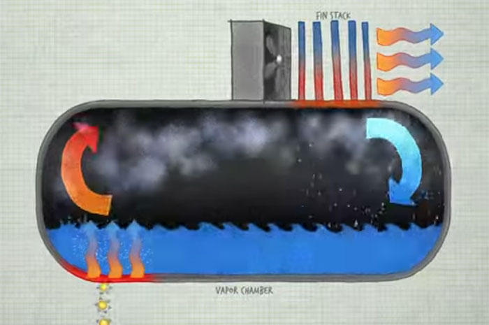
While we mull these concepts the video flashes progress made in Nvidia graphics card designs over the years and you can see familiar models and their cooling assemblies at various angles and in exploded views. With the talking heads discussing the increasing problem of power density and cooling, one starts to get the idea that Nvidia's upcoming graphics cards have been a bit of a challenge to cool.
Some sections of the Nvidia video turn more precisely to ponder over 'modern challenges' - thermal issues that the engineers and designers are facing now, or have faced recently with Ampere GPUs. In a section starting at about 6 minutes we are then treated to a view of the new 12-pin power connector which will replace the typical 2x 8 pin connectors on high-end boards.
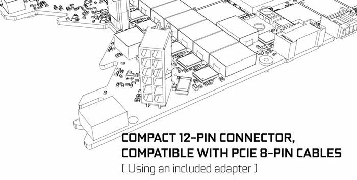
The animation showing the power connector replacement, which we know arrives with the introduction of the GeForce RTX30 series of consumer graphics cards, clearly shows the unusual shape of the PCB that features in this design.
Back in June we first heard about this pennant shaped PCB dubbed PG133. This unusually shaped PCB complements the double sided fan design of the RTX 30 Founders Editions. There is also supposed to be a more standard rectangular PCB dubbed PG132 for board partners to utilise versions of their typical cooling shrouds we have seen on previous gen graphics cards.
In its accompanying blog post Nvidia says that its engineers and designers have pondered over the following points to create cool and quiet GPUs that can reach their maximum potential:
- Thermal: A new, airflow-optimized cooling solution, redesigned to overcome existing constraints and move more air through the system for maximum cooling efficiency
- Mechanical: A stronger mechanical structure, including a new low profile leaf spring that leaves room for a back cover
- Electrical: A compact electrical design, with a new 12-pin power connector that allows more space for components and cooling, and is compatible with existing power supplies via an included adapter
- Product Design: A no-compromise, cohesive design that embraces the revolutionary thermal solution while beautifully harmonizing each element of the graphics card
As a reminder, Nvidia's GeForce Special Event will be live next Tuesday, 1st Sept.


