Intel held a Technology and Manufacturing Day event in Bejing, China yesterday. On stage various executives talked about advancements in Intel tech emanating from its manufacturing prowess and shared details of milestones that had been passed. Highlights included; power and performance updates for Intel's 10nm process, high-level plans for Intel's first 10nm FPGA, and an announcement that the industry's first commercially available 64-layer 3D NAND for data centre applications has shipped.

Intel's 10nm tech
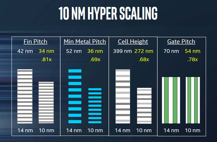
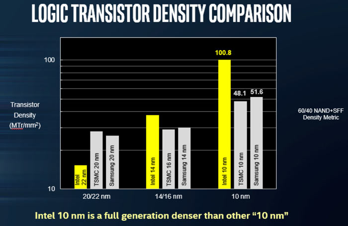
Intel Senior Fellow Mark Bohr took to the stage to assert that "Intel's 10nm is a full generation ahead of other 10nm technologies in terms of both transistor density and transistor performance". With the tightest transistor and metal pitches the greatest densities can be achieved. Intel Hyper scaling manufacturing technology facilitates up to 2.7x logic transistor density improvements compared to the company's 14nm and 10nm processes.

On stage Intel showed both a 10nm Cannon Lake wafer (pictured top, held aloft by Stacey Smith) and a 10nm ARM Cortex-A75 CPU wafer. The event attendees were told the 10nm Intel manufactured ARM cores could run at speeds in excess of 3GHz.
On a related topic, Intel wants to clear up 'node-naming confusion'. Many tech enthusiasts will be aware that not all 14nm chips, for example, are created equally. So Intel wants to "standardize on a common measure of transistor density that facilitates easy comparison across different manufacturers". However, one might assume other manufacturers won't want to play ball and fall in line with Intel formulated standards that make Intel chips look superior.

Intel plans to introduce 10nm process FPGAs. Codenamed Falcon Mesa, the new FPGAs "will offer new levels of performance to support the growing bandwidth demands of data centre, enterprise and networking environments". There's a Falcon Mesa fact sheet available to those interested in this technology (PDF).
64 layer TLC 3D NAND SSD
In China Intel also announced it was already shipping the industry's first 64-layer, triple level cell (TLC) 3D NAND SSDs for data centre applications. Such drives started shipping in early August but only to Intel's top tier customers. However, these new SSDs will be made broadly available before 2017 is out.


