TSMC
According to various reports, citing recent announcements by TSMC at the 2019 VLSI Symposium in Japan, and SEMICON West 2019 in San Francisco, TSMC has started to roll out optimised versions of its N7 process and provided info about a similarly upgraded N5 process. The new performance optimised versions of these processes will deliver 7 per cent higher performance over predecessors at iso-power. The N7P and N5P processes are not to be confused with the '+' suffixed processes which adopt EUV for a few critical layers.
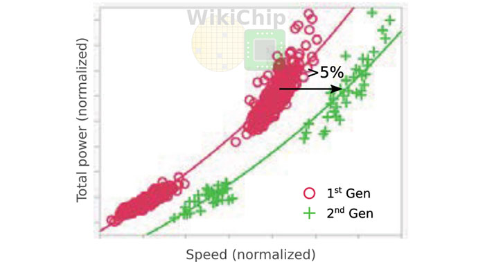
TSMC's N7P has started to roll out and is known internally as both '2nd generation 7nm' and '7nm year 2,' reports WikiChip. N7P can create optimised fully-IP compatible versions of N7 designs with added EOL and MOL optimisations. The optimisations result in device designers being able to choose between either 7 per cent performance improvement at iso-power, or up to 10 per cent lower power at iso-speed.

Like the N7P above, TSMC's N5P will be uses the same design rules and is fully IP-compatible with its predecessor (N5 in this case). The same optimisations work a bit better here, with the N5P designs being able to offer 7 per cent higher performance over N5 at iso-power, or 15 per cent lower power at iso-performance. N5P is expected to go live between late 2020 and early 2021.
Samsung
Currently Samsung is busy pumping out 7LPP (7 nm low power plus) chips, and has been doing so since last October. In April this year 7LPP was put into mass production and has been in high demand ever since. As with TSMC, Samsung never seems to take a breather and has been outlining its next steps with regard to optimisation and further node shrinks.

Samsung's 7LPP was the company's first process to use EUV, and its successors will use it more extensively, reports AnandTech. 6LPP is coming in H2 this year and has 10 per cent greater transistor density than 7LPP. Samsung's 6LPP is flexible in that it allows chip designers to re-use the IP they already might have on 7LPP or implement new 'smart-structures' in 6LPP for advanced feature support.
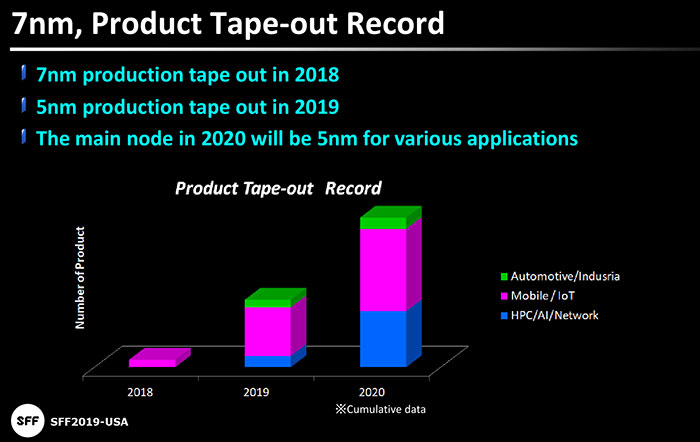
Things are certainly moving fast at Samsung as it has said that 5nm development is complete, and it sees 4nm development being completed before the end of this year. As for mass production scheduling, 6LPP is due to hit the fast lane in H2 this year, with 5LPP starting in H1 2020.

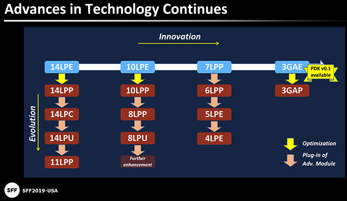
As you can see in Samsung's tech advances slide, its next major innovation will be to move to 3GAE for which it has already made product dev kits available.


