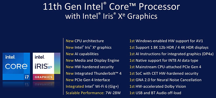
Most observers would agree that Intel hasn't had a great 2020. There was positive progress that earned it fair share of headlines like the readying of Tiger Lake processors with Xe graphics, and the unveiling of 10nm SuperFin technology, however investors looked elsewhere to make their money work and Intel shares have dipped 18 per cent in 2020.

CNBC reports that activist hedge fund Third Point has written a letter to Intel's board of directors requesting some changes. The letter became came to light on Tuesday and cause Intel's shares to rally 5 per cent, such is the considerable weight of Third Point's opinion and the likelihood Intel will take the points on board. For the record the hedge fund is estimated to hold a $1bn stake in Intel.
Highlights of the letter are a push for Intel to explore "strategic alternatives" after the chipmaker has lost market share to TSMC, Samsung and AMD. Of particular annoyance to the fund is Intel's loss of manufacturing leadership. To remedy this slide it could invest more in its manufacturing which could be important for US national security interests too.
Other business activities under scrutiny by the hedge fund are the Intel acquisitions that haven't paid off. I think it is good for tech giants to indulge in moonshoot and tangential technology projects but the business needs a certain percentage of wins from previous similar activity to convince investors that spending on such projects are worthwhile. The trouble is hedge funds like Third Point might be happy with a quick bounce – who knows how long they will hold their investment for.
Stacked Nanosheet Transistor advance
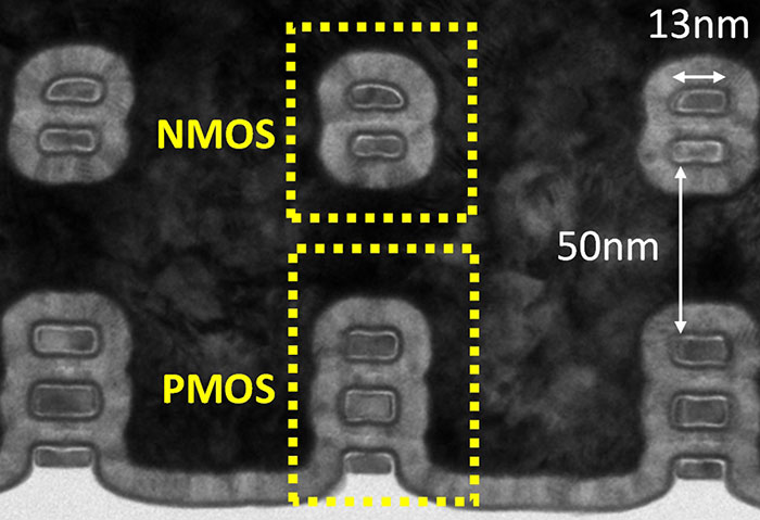
At the IEEE International Electron Devices Meeting (IEDM) this week Intel took the wraps off a new recipe for building stacked nanosheets which unify NMOS and PMOS transistors.
The IEEE Spectrum magazine reports that Intel's technique effectively cuts the footprint of a CMOS circuit in half, or to put it another way it can double the transistor density of resulting ICs. The source explains the new process as follows:
At its heart, the process is a modification of the steps involved in making nanosheet transistors. It starts with repeated layers of silicon and silicon germanium. This is then carved into a tall narrow fin, and the silicon germanium is etched away to leave a suspended set of silicon nanosheets. Ordinarily, all the nanosheets would go to form a single transistor. But here, the top two nanosheets are connected to phosphorous-doped silicon with the aim of forming an NMOS device, and the bottom ones to boron-doped silicon germanium to yield PMOS.

In this first iteration of the tech, the Intel research team has concentrated on making the technology manufacturing friendly. Once that process is smoothly polished it plans to turn to optimising the performance of Stacked Nanosheet Transistors. Rival semiconductor firms have proposed similar technologies before, sometimes dubbed Complementary FETs of CFETs, but Intel's proposals are the most refined and practical.


