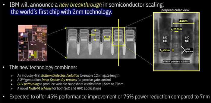
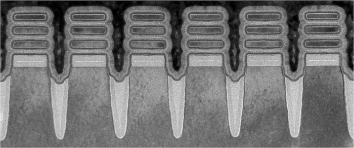
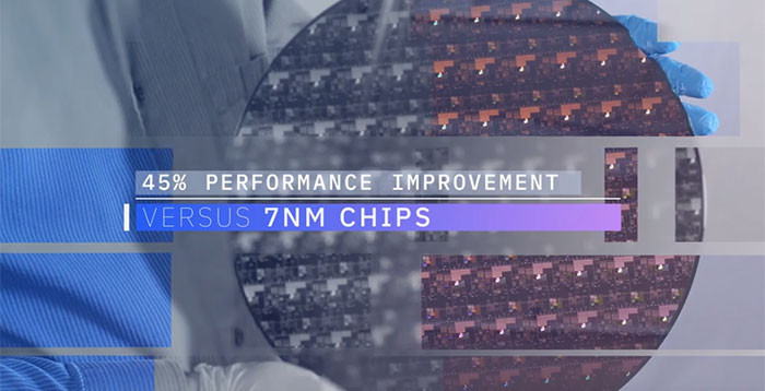
IBM has announced that it has created the world's first 2nm chip technology. It says that its new 2nm nanosheet technology will "propel major leaps forward in performance and energy efficiency". Working chip samples were designed and produced at IBM's research facility in Albany, New York. Backing up the "new frontier" claims with some numbers IBM asserts that the new 2nm parts will deliver the system maker's choice between "45 per cent higher performance, or 75 per cent lower energy use," compared to today's state-of-the-art 7nm processors.
If the above 7nm performance / energy use comparison isn't clear enough, IBM has some snappy bullet point potential benefits of its 2nm process to share:
- Quadrupling cell phone battery life, only requiring users to charge their devices every four days.
- Slashing the carbon footprint of data centers, which account for one percent of global energy use. Changing all of their servers to 2 nm-based processors could potentially reduce that number significantly.
- Drastically speeding up a laptop's functions, ranging from quicker processing in applications, to assisting in language translation more easily, to faster internet access.
- Contributing to faster object detection and reaction time in autonomous vehicles like self-driving cars.

Another illustration of the potential of 2nm comes from the simple explanation that the new nanosheet process enabled chip designers to pack 50 billion transistors into "a chip the size of a fingernail". That isn't a metric I would have chosen but the TSMC N7 Nvidia A100 GPU with 54 billion transistors measures 826mm2, about a 29mm square – quite a lot of fingernails.

What does this advancement mean to PC enthusiasts? IBM says now that it has pioneered this technology in its labs using the popular ASML machinery, it "shouldn't be too long" until chips can be mass-produced using 2nm nanosheet technology. Remember the recent Intel Engineering the Future webcast in March? At that event Intel mentioned many important things about chip manufacturing, but one of the key announcements were the new R&D partnerships with Microsoft and IBM (IBM logic and packaging). Still I would expect it to be some years before this IBM 2nm nanosheet technology (or a close relation to it) is used in consumer components / devices.


