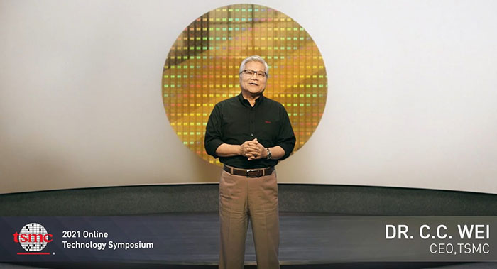
At its 2021 Technology Symposium, TSMC Chief Executive CC Wei said that the firm has started construction of chip making facilities in Arizona, US. Wei said that TSMC has allocated US$12 billion to the project. The Arizona plans are currently for a chip making factory which will deliver 5nm output in the US with mass production likely to be achievable by 2024.

Reuters explains that TSMC, and Samsung, have recently been lured to the US with $54 billion in subsidies for the chip industry passing though the late stages of US government approval at this time. The news site adds that TSMC could build on a successful venture and expand its Arizona facilities to as many as six factories over the next 10 to 15 years.
A press release from TSMC sums up the firm's latest innovations highlighted at its 2021 Technology Symposium, which comes to a close later today. During the online only event TSMC engineers, researchers, and scientists outlined some of the following; TSMC 3DFabric advanced packaging and chip stacking technologies, as well as info on the N5, N6RF, N4, N5A, and N3 process nodes.

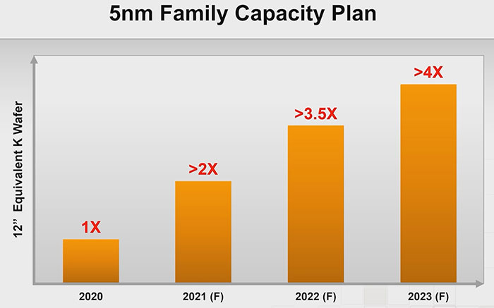
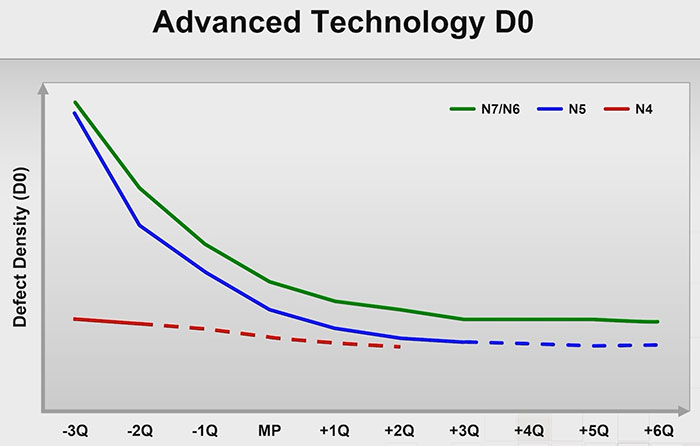
TSMC has been mass-producing N5 parts since 2020, and it is pleased to say that its defect density is improving faster than what it managed with N7. N6RF is a modified N6 process technology with optimisations for 5G radio frequency (RF) and Wi-Fi 6/6e solutions. As well as offering 16 per cent better performance than prior gen RF transistors, the new solution offers "significant power and area reduction for 5G RF transceivers," according to TSMC. Of course, power efficiency and mobile networking performance is all-important to portable devices like smartphones.

N4 is an enhancement of N5 which will "improve performance, power efficiency and transistor density along with the reduction of mask layers and close compatibility in design rules with N5". N4 risk production is scheduled for Q3 this year.
The new N5A process is aimed at "automotive applications such as AI-enabled driver assistance and the digitization of vehicle cockpits". N5A is founded on the logic density of N5 "while meeting the stringent quality and reliability requirements of AEC-Q100 Grade 2 as well as other automotive safety and quality standards," explains TSMC. The first N5A parts should be rolling off the production lines in Q3 next year.
TSMC reckons its N3 technology will be "the world’s most advanced," when it hits volume production in H2 2022. This FinFET transistor architecture will offer a design choice between 15 per cent better performance or 30 per cent lower power usage vs N5, as well as a 70 per cent logic density gain.

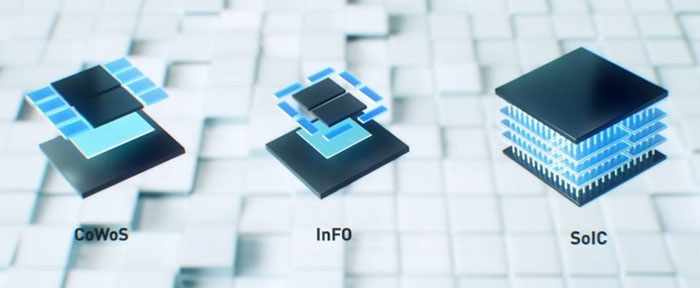
Last but not least, TSMC said that it is continuing to expand its 3DFabric family of 3D silicon stacking and advanced packaging technologies for both high-performance and mobile solutions. This info ties in with AMD's 3D V-Cache announcement yesterday. AMD said that it will be debuting some of its highest-end processors featuring 3D chiplets at the end of 2021 using chiplet and advanced 3D stacking tech created in collaboration with TSMC.


