Introduction
NVIDIA introduced its new high-end GPU architecture with the release of the GeForce GTX 280 graphics card in June of this year, closely followed by the second member of the family, GeForce GTX 260, a week or so later.
Recently, though, NVIDIA added to the GTX 200 family by launching another GTX 260, this time equipped with 216 cores and commensurately more filtering and fillrate power.
The purpose of this HEXUS.help guide is to explain how the current GTX 200 family stack up with respect to clock-speeds and, be they core, shader, clusters or memory pathways.
Architecture overview of GeForce GTX 280

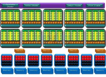
The above diagram shows a high-level, simplified view of a GeForce GTX 280 GPU. NVIDIA packs in 10 texture-processing clusters, compared with eight in high-end GeForce 8-series and 9-series GPUs. Each cluster is sub-divided into three streaming multiprocessors (up from two with 8-series and 9-series), though each SM has eight processing cores, just like the previous architectures.
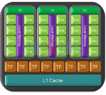
What that means is that each cluster has 24 processing cores (three blocks of eight), making a card-wide total of 240.
For a GeForce GTX 280, the cores operate at 1,296MHz, which, when multiplied by the 240 cores that can each process three instructions per clock cycle, brings total shading power of 933GFLOPS (1,242 x 240 x 3).

A larger view shows the three sets of eight 'cores'. Further, each cluster also amalgamates eight texture-filter portions that, between them, can filter eight bilinear pixels or four 16-bit floating-point pixels per clock cycle.
The eight ROPs, arranged in blocks of four, are then each attached to the card's memory via a 64-bit memory channel, meaning a card-wide 512-bit interface that hooks up to GDDR3 memory, usually operating at 2,214MHz. Do the math and you'll see that the GPU has around 141.7GB/s of bandwidth available to it (512/8 (to convert bits to bytes) x 2,214)
GeForce GTX 280 is the culmination of NVIDIA's design excellence and GeForce GTX 260 - 192- and 216-core - are both derived from it.
GeForce GTX 260 - 192/216-core
These GPUs use an identical underlying architecture with respect to shading, processing, filtering and memory bandwidth. The differences lie with how NVIDIA qualifies boards and removes performance-enhancing features. A table will help explain the differences.
| Graphics cards | NVIDIA GeForce GTX 280 240-core | NVIDIA GeForce GTX 260 896 192-core | NVIDIA GeForce GTX 260 216-core |
|---|---|---|---|
| PCIe | PCIe2.0 |
||
| GPU clock | 602MHz |
576MHz |
576MHz |
| Shader clock | 1,296MHz |
1,242MHz |
1,242MHz |
| Memory clock (effective) | 2,214MHz |
1,998MHz |
1,998MHz |
| Memory interface, size, and implementation | 512-bit, 1,024MB, GDDR3 |
448-bit, 896MB, GDDR3 |
448-bit, 896MB, GDDR3 |
| Memory channels | 8 |
7 |
7 |
| Memory bandwidth | 141.7GB/sec |
111.90GB/sec |
111.90GB/sec |
| Manufacturing process | TSMC, 65nm |
||
| Transistor count | 1,408m |
1,408m |
1,408m |
| Die size | 576mm² |
576mm² |
576mm² |
| DirectX Shader Model | DX10, 4.0 |
||
| Vertex, fragment, geometry shading (shared) | 240 FP32 scalar ALUs, MADD dual-issue (unified) |
192 FP32 scalar ALUs, MADD dual-issue (unified) |
216 FP32 scalar ALUs, MADD dual-issue (unified) |
| Clusters of SPs | 10 |
9 |
8 |
| Peak GFLOPS | 933 |
715 |
805 |
| Data sampling and filtering | 80ppc address and 80ppc bilinear (8-bit integer)/40ppc FP16 filtering, max 16xAF |
64ppc address and 64ppc bilinear (8-bit integer)/32ppc FP16 filtering, max 16xAF |
72ppc address and 72ppc bilinear (8-bit integer)/36ppc FP16 filtering, max 16xAF |
| Peak fillrate Gpixels/s | 19.264 |
16.128 |
16.128 |
| Peak Gtexel/s (bilinear) | 48.16 |
36.864 |
41.472 |
| Peak Gtexel/s (FP16, bilinear) | 24.09 |
18.432 |
20.736 |
| ROPs | 32 (8x4) |
28 (7x4) |
28 (7x4) |
Analysis
Knowing that the GeForce GTX 260 is now divided into 192- and 216-core models and that the architecture is based on clusters of 24, the old GTX loses two clusters and the new GTX one cluster when compared to 10-cluster GeForce GTX 280. You can see how this affects the GFLOPS throughput of each of the GPUs.
It would be reasonable to assume that NVIDIA's screening process determines which GPUs don't quite have 10 operational clusters and then downmarks them to either GTX 260 eight- or nine-cluster SKUs. Further, the bilinear fillrate is different on each GPU because the filtering units are associated with the clusters.
Memory bandwidth is also down on the two GTX 260s, to the same degree, because they use seven 64-bit memory channels instead of eight. A knock-on effect of populating one less memory channel is that one fewer memory device (DRAM) can be used, and therefore GTX 260s ship with seven 1,024Mbit modules instead of eight, leading to a card-wide 896MB as opposed to the GTX 280's 1,024MB.
Appreciating the lopping off of clusters and memory channels/ROPs, GeForce GTX 260s also feature slower clock-speeds on all counts, too, meaning that a GTX 280 is greater in both architecture and clocks - reducing its speeds down to GTX 260 levels would still make it faster in the majority of gaming titles.
Overview
GeForce GTX 280 is the range-topping architecture debuted by NVIDIA nearly six months ago. GeForce GTX 260 loses out in a couple of important ways, most notably with respect to basic architectural lop-offs and clockspeeds, so it can be summarised as follows:
GeForce GTX 280 has 240 cores, spread over 10 cluster units, eight 64-bit memory channels, eight ROP blocks, and operates at 612MHz core, 1,296MHz shader, and 2,214MHz memory.
GeForce GTX 260 216-core loses one 24-core shading/cluster unit, one 64-bit memory channel and associated four-ROP block. It operates at slower clocks of 576MHz core, 1,242MHz shader, and 1,998MHz memory.
GeForce GTX 260 192-core loses two 24-core shading/cluster units, one 64-bit memory channel and associated four-ROP block. It operates at slower clocks of 576MHz core, 1,242MHz shader, and 1,998MHz memory.
Understanding the architecture differences, it is reasonable to assume that the GTX 260 216-core provides 80-85 per cent of the GTX 280's performance and the GTX 192-core provides somewhere in the region of 70-75 per cent. At the time of writing, a stock-clocked GTX 280 costs around £320, a GTX 260 216-core some £230, and a GTX 260 192-core around £200. Basic maths tells the best bang4buck, then, is probably the 192-core GTX 260.
Just take a look at the GFLOPS (shading) and memory-bandwidth numbers as rough-and-ready reckoners of overall performance once games are limited by the GPU and not CPU, ideally when set to high resolutions with lots of image-quality enhancement.
Customers need to appreciate the technology and trade-offs between the GeForce 200 family and then base a buying decision around it. NVIDIA's used the twin salvo of clock and architecture cuts to traverse the range, and, we feel, that it has segmented the range quite well.


