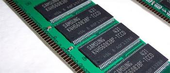
Firstly, DDR stands for Dual Data Rate and is the replacement for SDRAM. The best analogy we have come across for how DDR works is: If the memory is visualised as a bicycle pump, SDRAM “pumps” push data into the “tyre” each time the barrel of the pump is pressed down, whereas DDR pushes data both on the downstroke and the upstroke of the barrel so filling the “tyre” at twice the speed.
DDR has a data rate of 200/266/333/400 MiB/s compared to DDR2 which has a data rate of 400/533/667 MiB/s, it is clear to see that from a speed point of view DDR2 continues where DDR leaves off. The table below courtesy of the Corsair website helps illustrate other notable differences.
| DDR | DDR2 | |
|---|---|---|
| Data Bus | 64 bits | 64 bits |
| Data Rate | 200/266/333/400 MiB/s | 400/533/667 MiB/s |
| Bus Frequency | 100/133/166/200 MHz | 200/266/333 MHz |
| DRAM Frequency | 100/133/166/200 MHz | 100/133/166 MHz |
| Package Type | TSOP-II | FBGA |
| Densities | 256MB 512MB 1GB | 256MB 512MB 1GB |
| Voltage | 2.5V | 1.8V |
| Prefetch Size | 2 bits | 4 bits |
| Burst Length | 2/4/8 | 4/8 |
| CAS Latency | 1.5, 2, 2.5 | 3+, 4, 5 |
| Write Latency | 1T | Read Latency -1 |
Package type refers to the physical layout of modules. DDR memory modules are built using the standard TSOP-II architecture (Thin Small Outline Package) where transistors are laid out in grid formation; DDR2 uses a newer layout named FBGA (Fine Ball Grid Array) which allows a higher transistor count in the same physical package.

DDR and DDR2 are not compatible with each other. Where DDR has the TSOP package the module interfaces with the slot via 184 pins mounted on the side of the module, DDR2 uses 240 pads mounted on the underside of the module which interface with the slot. The FBGA architecture used in DDR2 allows for much more efficient placement of traces and pads, it being possible to run traces closer to the original source. Both modules are 5.25” in length and to prevent end users inadvertently plugging DDR into a DDR2 slot or vice versa the fitment slot is located differently on the two types.
Some other new technologies are incorporated into DDR2 also. With DDR, excess signal noise, reflected signals and other interference is eliminated by motherboard based transistors. DDR2 differs in that these terminating transistors are removed from the motherboard and are instead built into each memory module, allowing excess noise to be eliminated faster, this technology is called On Die Termination (ODT).
Another method of increasing signal integrity is OCD (Off Chip Driver calibration), which helps maintain the signal by smoothing voltages and supplying a reference voltage and is again built into the modules. Posted CAS and Additive Latency both aid in preventing data collisions within the module whilst allowing a greater number of read/write transactions per clock cycle increasing efficiency.
Two other things to take from the table are the increased CAS latency (CL) and reduced operating voltage. The change in CAS latency is required to offset the speed increase. Whether this increase greatly affects performance remains to be seen. Early samples did suffer from higher latency and in some cases were slower than their DDR relatives, however technology has moved on since then and newer models are running with much lower latencies and with the increased performance this brings. The operating voltage required by DDR2 modules is much reduced meaning less voltage is required to read from and write to the memory, another indication of increased efficiency.
CAS stands for Column Address Strobe, and Latency is defined as the amount of time between a stimulus and a response; to use another analogy: a RAM module can be compared to a spreadsheet, but with “memory” cells in place of numbers and formulae, with each cell possessing a cell address derived from its column and row position. As expected and inline with the analogy there also exists RAS latency or Row Address Strobe. To fetch data the chipset accesses the desired row of the memory “spreadsheet” by placing the required cell address on the memory address pins and switching on the RAS signal. The time in clock cycles taken to process this instruction is known as RAS to CAS delay, once complete the column address is fed into the address pins and the CAS signal made active to allow the correct column of your memory spreadsheet to be accessed, once again a few clock cycles pass before the data is available on the memory pins.
This delay between addressing the column pins and the data being available is CAS latency. With CAS 2, two clock cycles pass before the data is ready and with CAS 3, three clock cycles pass. This is not to say, however, that a CAS 2 module is a third faster than CAS 3, as other factors also affect how quickly data is retrieved. In essence, however, lower CAS latencies generally mean better performance as data can be accessed in a shorter amount of time.
DDR2 has been around for over 12 months on graphics cards, but the base standard and architecture differs from that used on a motherboard module. At present DDR2 is only supported by Intel based systems with AMD expected to launch compatible models sometime during 2006.
In summary, faster data rates, increased frequencies, expected support by both major CPU manufacturers and a more power efficient module, all these factors point to increased use by desktop PC owners of DDR2, and with latencies falling all the time DDR2 looks increasingly certain to be the future of memory design.


