A peek under the Intel Core i7-5960X Integrated Heat Spreader

by Mark Tyson on 29 July 2014, 11:15

Tags: Intel (NASDAQ:INTC)

Quick Link: HEXUS.net/qacg4j

Add to My Vault: x

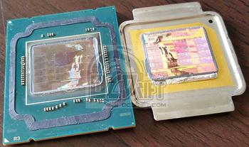
Malaysian overclocking enthusiast Kevin Owi (Owikh84) has de-lidded what he claims to be Intel's upcoming Core i7-5960X chip. He wanted to take a peek at what the processor would look like after its Integrated Heat Spreader (IHS) was removed and find out more about the improved Thermal Interface Material (TIM) that Intel boasts about. I've embedded his main feature picture directly below.

The Intel Core i7-5960X is one of Intel's upcoming 'Haswell E' processors so Owihk84 did well to get his hands on it and then take the risk of de-lidding this purported US$999 part for the curiosity of the PC enthusiast community. This Core i7-5960X is going to be the flagship of the trio of initial Haswell E launch processors, boasting 8 cores and 16 threads, 20MB of L3 cache and a regular/turbo clock speed of 3.0GHz/3.3GHz.

Looking closely, the 22nm chip pictured above, appears to have 12 core modules (the 3x4 grid) so four of these must be disabled. That's still going to consume a lot of power in a small area with a purported TDP of 140W. So the TIM will be very important to make the best use of the cooling system you employ to get the heat out of a system based on one of these chips.

Owikh84 removed a strong layer of conductive epoxy which Intel had used to fix the Integrated Heat Spreader (IHS) to the chip die. This 'solder' is said to offer much better conductivity than the TIM used in the likes of the Intel Core i7-3770K, 4770K, and 4790K for example.

The chip you see under the knife in this picture is expected to be officially released sometime in September this year. When this chip does become official we won't be putting it under the knife but it will definitely be put under the HEXUS benchmark microscope.


HEXUS Forums :: 11 Comments

Login with Forum Account

Don't have an account? Register today!
That's some fairly dramatic die harvesting! I wonder if the 6 core versions will be native 6 core dies?

Epoxy!=solder though. My experience with thermal epoxy shows it to be fairly similar to TIM in thermal performance but very much more permanent.
There does seem to be a lot of confusion over whether it's an epoxy or a solder.
It looks more like epoxy/TIM to me, going by the included image.

Edit: The source article says
soldered the chip’s die to the IHS with a strong epoxy
Which is a bit like saying ‘screwed together with a staple’ - they're two fundamentally different bonding techniques. But I guess something is just lost in translation.

Epoxy uses epoxy resin which cures through a chemical process. Soldering uses a metal alloy which is heated to make it fluid, and sets by cooling.
watercooled
That's some fairly dramatic die harvesting! I wonder if the 6 core versions will be native 6 core dies?

Epoxy!=solder though. My experience with thermal epoxy shows it to be fairly similar to TIM in thermal performance but very much more permanent.

Ivy Bridge-E had 12-core and 6-core die variants, so 4960X was a native 6-core, whilst the 4820K was die harvested. I'd guess they are going the same way with Haswell-E since they are on the same process node.

By contrast Sandy Bridge-E was 4 and 8-core variants, so the 3960X was an 8-core, die harvested part and the 3820 was a native 4-core.
It's nothing terribly unusual, I was just passing comment; it's not a very high-volume part after all.

However, I half-expected a native 8 or 10 core die for Haswell-E considering we had:
SNB-E: 4, 8
IVB-E: 6, 10, 15 (the 12C is actually a 15C die IIRC)
But HSW-E is now 6??, 12, ??? - see what I mean?

Assuming there is a smaller die than 12C in HSW-E, this would imply it's a 6C, which is a big jump from 12 cores.

The IVB-E cores were arranged in columns, so the 10C die was similar to the 15C with one side sliced off, and with the 6C being arranged slightly differently. Time for some complete speculation; looking at the picture in the article, the HSW-E die looks very much like the three-column 15C IVB-E die. With one of those columns sliced off, you'd have an 8C die (assuming it's designed that way OFC).

However something else has just occurred to me, IVB-EX 15C was already 541mm2 i.e. massive (and probably not too far off reticle size), and Haswell cores are larger than IVB. People are talking about 18C dies, but how big a die would that mean?? Even looking at the picture, that die is seriously huge; I'm not sure how much room there is left under the heatspreader for another 6 cores + cache!

It will be interesting to watch this, for sure…