First pictures of Nvidia GM107 'Maxwell' GPUs emerge

by Mark Tyson on 6 February 2014, 10:41

Tags: NVIDIA (NASDAQ:NVDA)

Quick Link: HEXUS.net/qacaib

Add to My Vault: x

Video card oriented site VideoCardz has rustled up the web's first pictures of the upcoming Nvidia 'Maxwell' GPU range. Also the site fills us in on some details of what the first cards with these chips will offer to end users when they are launched installed on video cards in less than a fortnight's time.

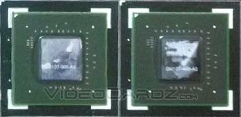
In the picture you can see two Nvidia GM107 chips side-by-side in a tray, presumably on the way to being incorporated into fully assembled graphics cards. VideoCardz says that the new chip is a hybrid of the GK106 and GK107 designs as it can have the same CUDA count as a GK106 which is combined with the 128-bit memory bus of the GK107. It is also noted that the die area of the new Maxwell chips detailed here offers a 30 per cent reduction on the GK106.

The new GM107 chips will be able to be employed upon graphics cards which don't require any power connectors. VideoCardz says that this is due to the "footprint and power consumption will be dramatically lower than any Kepler GPU". Note the GM107-400 TDP in the chart below.However these first Maxwell chips will not be made upon the 20nm process as TSMC isn't ready at this time to do so, these GM107 chips are made on the 28nm process. It is expected that when the first 20nm Maxwell chips are manufactured - that will mark the start of the GeForce 800 series for add-in video cards.

Two variants of the GM107 are known of at this time; the GM107-300 with 768 CUDA cores and the GM107-400 with 960 CUDA cores. These will power the Nvidia GeForce GTX 750 and Nvidia GeForce GTX 750 Ti respectively (both due on 18th Feb). You can see further differences to these chips in the table from VideoCardz embedded above.


HEXUS Forums :: 10 Comments

Login with Forum Account

Don't have an account? Register today!
Further details of the Nvidia GeForce GTX 750 and Nvidia GeForce GTX 750 Ti can be found thanks to some information/screens from a pair of AIC branded cards being published. The referenced UK Gaming Computers source article has been taken down but TechPowerUp poached some pictures.

The thing is though the GK106 is probably a 256 bit part with more ROPs,but is artificially hobbled - even the power limits are very low compared to other SKUs. Nvidia did this before with the GTS450. However,they probably had more than enough GK104 salvage parts and this is why we saw the GTX660TI and GTX760.

The GM107 looks like a fully enabled die,so unless there is an equivalently specced Kepler die,we cannot say whether Maxwell is much lower power and/or more transistor efficient anyway.

Its nice the GTX750TI is bus powered,however remember there was the odd bus powered HD7850 too(!).

It will be interesting to see how the GTX750TI and GTX660 compare at 1920X1080 though especially with AA.
Passive GM107-400 would be interesting. Might put my Radeon 260 plans on hold to see how this shakes out.
It might not boost that much if passively cooled though.

OTH,if the power limits are like with my GTX660,ie,quite low,it probably will be OKish.
So. Late, 28nm, and launching the LOW end parts first? Something doesnt seem right at the NV house…

It does however amuse me they are finally taming the fusion reactor that was fermi down to something reasonable.