Samsung, not just a devices maker but a significant player in the semiconductor industry, has announced that it has begun mass production at its new EUV manufacturing line. At its new dedicated extreme ultraviolet (EUV) lithography facility,dubbed V1, it will be producing both 7nm and 6nm EUV chips. Probably of most interest to HEXUS readers is that it has previously been confirmed that Nvidia has booked manufacturing its next-generation GPU at this facility and Samsung will be producing "substantial" numbers of them.
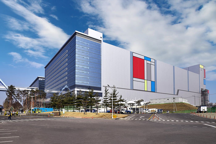
The new dedicated EUV V1 line is operational within Samsung's plant in Hwaseong, South Korea. As mentioned above, it will be outputting both 7nm and 6nm chips. Samsung plans to adapt the line to eventually produce chips with features as small as 3nm. No timescale is mentioned for that further halving of transistor size.
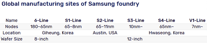
By the end of 2020 Samsung will have invested US$6bn in its V1 line. It will continue to ramp up production on V1, and coupled with its smaller S3 line aims to triple is 7nm and smaller output capabilities by the end of the year. An overview of Samsung's foundry production facilities at the time of writing can be seen charted below.
Turning to timings, for those of you champing at the bit for new Nvidia GPUs, Samsung says that the first V1 line products will be delivered to customers in Q1 this year. For 'customers' I would read that to mean Samsung's business customers like Nvidia Corp. Nvidia is hosting its annual GTC in San Jose from 22nd to 26th March, where it is expected to unveil Ampere GPUs, as well as a load of robots.
This 7nm and 6nm mass production capacity from Samsung will help it become more competitive throughout 2020 with contract manufacturing behemoth TSMC - vying for business from the likes of AMD, Apple, Nvidia, and Qualcomm as well as many lesser known industrials.