So far we have only seen limited hardware releases packing HBM1 or HBM2 memory but sk Hynix and Samsung are already working on HBM3 and other memory technologies and teased this fact at the current Hot Chips Symposium in Cupertino. According to slides published at Hot Chips, the next generation HBM will offer improved density, bandwidth, cost, power efficiency, and more.
AMD used HBM1 in its Fury range of graphics cards. Nvidia used HBM2 in its Pascal-based Tesla P100 accelerator. For HBM3, perhaps AMD will be the first company to make a shipping product using the new memory, as its roadmap says the Vega architecture GPU (with HBM2) will be followed up with the Navi GPU with 'NextGen Memory'.
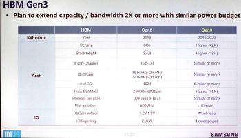
In a more specific information release, at the recent IDF, Samsung published a slide showing HBM3 will offer more than twice the density and bandwidth of HBM2. It directly compares HMB2 and HBM3. Check out the table below to easily see the advances.
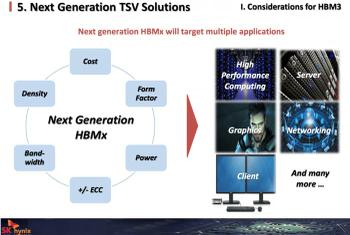
In other Hot Chips memory news, sk Hynix said it was looking forward to expanding HBM tech to HPCs & Servers, Networking & Graphics Card products, and Client Desktops and Laptops. For these purposes HBM2 memory will be available in sizes up to 32GB (4 stacks of 8 Hi modules).
Cheaper chips – GDDR6 and 'Low Cost HBM'
At the more affordable end of the new memory technology market Samsung detailed a couple of interesting new developments. At Hot Chips it showed off slides illustrating progress with developing GDDR6 and with a new type of HBM dubbed 'Low Cost HBM'.
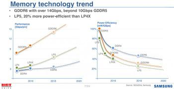
GDDR6 is expected to arrive as the successor to GDDR5X in 2018. Currently GDDR5X can achieve 10Gbps with that bar being raised to 12Gbps shortly. As you can see from the Samsung slide, above, GDDR6 will offer a bandwidth of about 15Gbps from the start and greater power efficiency.
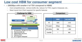
Samsung's plans for Low Cost HBM are interesting. It will remove the buffer die, and reduce the number of TSV (through-silicon via) connections, interposers and more, for cost competitiveness. However, on a positive note, it will offer 50 per cent improved pin speeds. As you can see from the slide, above, while HBM2 offers around 256GB/s bandwidth the Low Cost HBM will not be that far behind with approx 200GB/s. Low Cost HBM will be an undisclosed fraction of the price of HBM2 and, importantly, it targets the mass market.
Sources: VideoCardz, TweakTown 1, 2.


