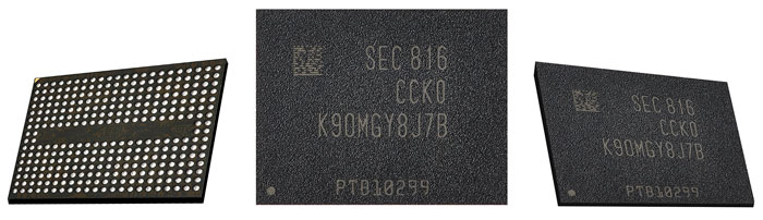
Samsung's strides in memory manufacture continue at a pace as today it announces that it has started mass production of its 5th generation V-NAND flash. This memory is made using a stack of memory chips, more precisely 96 layers of 3D charge trap flash (CTF) cells. Samsung's previous generation V-NAND employed 'just' 64 layers. The new chips deliver both greater density and performance improvements.
In its press release about the 5th gen V-NAND Samsung starts by revealing the performance potential of the new flash memory. It says that the chips, the first to use the 'Toggle DDR 4.0' interface, can transfer data from storage to memory at 1.4Gbps, a 40 per cent increase compared to their 64-layer predecessors. Additionally, the new V-NAND "has the fastest data write speed to date at 500-microseconds, which represents about a 30 per cent improvement over the write speed of the previous generation". Last but not least, the response time to read-signals has been significantly reduced to 50-microseconds.
Further good news about the 5th gen V-NAND from Samsung is that, while it ups the performance, its energy efficiency "remains comparable to that of the 64-layer chip." This is due to Samsung being able to lower the operating voltage from 1.8 volts to 1.2 volts.
In a statement alongside this 5th gen V-NAND announcement, Samsung Electronics EVP of Flash Product and Technology, Kye Hyun Kyung, said "In addition to the leading-edge advances we are announcing today, we are preparing to introduce 1-terabit (Tb) and quad-level cell (QLC) offerings to our V-NAND lineup that will continue to drive momentum for next-generation NAND memory solutions throughout the global market."
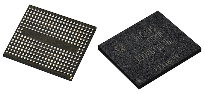
Back to the new 5th gen V-NAND, and Samsung says that it is quickly ramping up production with the first 96 layer parts being 256Gb TLC dies. It expects the chips to be employed in sectors as diverse as supercomputing, enterprise servers and premium smartphones in coming months.